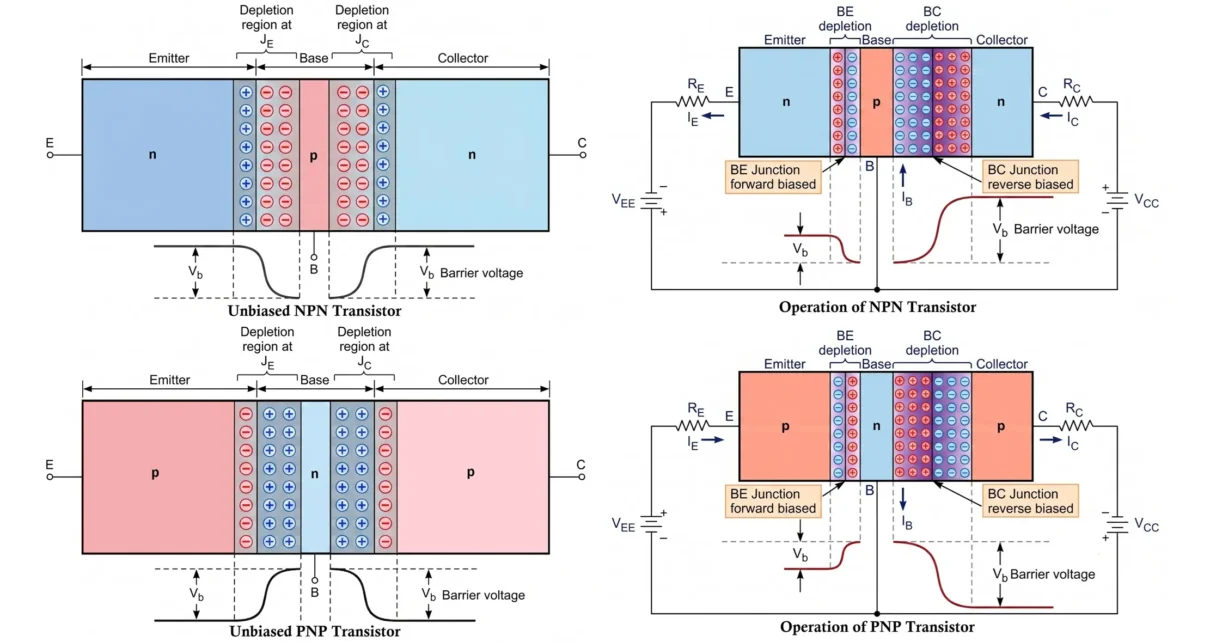
Let’s explore the biasing and operation of NPN and PNP transistors to understand how proper transistor biasing controls current flow, establishes the operating point (Q-point), and enables a bipolar junction transistor (BJT) to function as an amplifier or an electronic switch.
The operation of a transistor depends on the biasing of its two PN junctions Emitter-Base (EB) Junction and Collector-Base (CB) Junction. Depending on whether these junctions are forward or reverse biased, a transistor can operate in four regions: Active Region, Saturation Region, Cut-off Region, and Reverse (Inverse) Active Region. The active region is mainly used for signal amplification, while the saturation and cut-off regions are commonly used in switching circuits.
The operating principles of NPN and PNP transistors are the same, but the direction of current flow, movement of majority charge carriers, and voltage polarities are opposite. In an NPN transistor, electrons are the majority charge carriers, whereas in a PNP transistor, holes carry most of the current.
Understanding transistor biasing is important because improper biasing can reduce performance, cause signal distortion, or prevent the transistor from operating correctly. Proper biasing provides stable operation, better efficiency, improved thermal stability, and reliable circuit performance.
Related Articles:
- Bipolar Junction Transistor (BJT): Construction and Working
- MOSFET: Metal Oxide Semiconductor Field Effect Transistor
- JFET Junction Field Effect Transistors Working and Applications
- IGBT Full Form, Symbol, Construction, Working and Applications
- UJT Unijunction Transistor Symbol, Construction & Working
- Difference Between Photodiode, Phototransistor and Photoresistor
- Types of Transistors: Classification (BJT, JFET, MOSFET & IGBT)
Principle of Operation of Bipolar Junction Transistor
A Bipolar Junction Transistor consists of two PN junctions connected back-to-back, forming three semiconductor regions known as the Emitter, Base, and Collector. Since current conduction involves both electrons and holes, it is called a bipolar transistor.
The emitter is heavily doped to inject a large number of charge carriers into the base. The base is made extremely thin and lightly doped so that only a small percentage of these carriers recombine within it. The collector is moderately doped and physically larger than the emitter because it must collect most of the injected carriers and dissipate more heat.
When appropriate bias voltages are applied:
- The Emitter-Base (EB) junction is forward biased, allowing majority charge carriers to enter the base region.
- The Collector-Base (CB) junction is reverse biased, creating an electric field that quickly attracts these carriers into the collector.
Since the base is extremely thin, only a very small portion of the injected carriers recombine with opposite charge carriers in the base. This small recombination current forms the base current (IB), while the remaining carriers are collected by the collector, producing a much larger collector current (IC).
The emitter current is therefore the sum of the collector current and the base current.
IE = IC + IB
Since the base current is very small compared to the collector current, a tiny change in the base current can control a much larger collector current. This property makes the transistor an excellent current amplifier.
The collector current is approximately proportional to the base current and is given by:
IC = β IB
- IC = Collector Current
- IB = Base Current
- β (Beta or hFE) = DC Current Gain of the transistor
The value of β typically ranges from 20 to 500 depending on the transistor type and manufacturing process.
This simple current-control mechanism forms the basis of transistor operation in amplifiers, oscillators, switching circuits, voltage regulators, digital logic circuits, and thousands of other electronic applications.
Unbiased NPN and PNP Transistors
An unbiased transistor is a Bipolar Junction Transistor (BJT) in which no external DC voltage is applied to any of its terminals. In other words, the emitter, base, and collector are left electrically unconnected to any power supply. Since neither the emitter-base (EB) junction nor the collector-base (CB) junction is forward or reverse biased, the transistor remains in its natural equilibrium state and no significant current flows through it.

Both NPN and PNP transistors behave similarly in the unbiased condition. Although the transistor consists of two PN junctions, these junctions prevent the free movement of majority charge carriers because built-in electric fields are already present at each junction. As a result, the transistor remains in the OFF state until an external bias voltage is applied.

Studying the unbiased transistor helps in understanding how depletion regions and barrier potentials are naturally formed inside the semiconductor material before any external voltage is connected.
Formation of Depletion Regions
When the P-type and N-type semiconductor materials are joined during transistor fabrication, electrons from the N-region diffuse into the P-region, while holes from the P-region diffuse into the N-region. This movement of charge carriers leaves behind fixed ionized donor and acceptor atoms near each junction, creating a region depleted of free charge carriers known as the depletion region.
The depletion region produces an internal electric field that opposes further diffusion of charge carriers. This built-in electric field establishes an internal voltage known as the barrier potential or junction potential, which prevents additional majority carriers from crossing the junction under unbiased conditions.
Because a BJT contains two PN junctions, two depletion regions are formed:
- Emitter-Base (EB) Junction Depletion Region
- Collector-Base (CB) Junction Depletion Region
Distribution of the Depletion Region
The depletion region does not extend equally into both semiconductor regions. It always penetrates more deeply into the lightly doped region and less into the heavily doped region. This occurs because equal amounts of positive and negative charges must exist on both sides of the junction.
In a typical transistor:
- The emitter is heavily doped.
- The base is extremely thin and lightly doped.
- The collector is moderately doped and physically larger than the emitter.
Therefore:
- At the Emitter-Base junction, the depletion region extends only slightly into the heavily doped emitter but penetrates much farther into the lightly doped base.
- At the Collector-Base junction, the depletion region again extends mainly into the base because it is lightly doped. Since the collector is less heavily doped than the emitter, the depletion layer at the collector junction is usually slightly wider than that at the emitter junction.
This unequal distribution of the depletion regions plays an important role in the efficient operation of the transistor once external biasing is applied.
Barrier Potential of a Transistor
Every PN junction possesses a built-in voltage called the barrier potential (also known as the built-in potential or junction voltage). It is the minimum voltage that must be overcome before majority charge carriers can cross the junction and conduction can begin.
Since a transistor contains two PN junctions, both the emitter-base and collector-base junctions have their own barrier potentials. Under unbiased conditions, these internal voltages prevent the free flow of charge carriers across the junctions.
For a silicon transistor, the barrier potential across each PN junction is approximately: VBE ≈ 0.7 V
For a germanium transistor, the barrier potential is much lower: VBE ≈ 0.3 V
These values are approximate and may vary slightly with temperature, semiconductor material, and manufacturing process.
Current Flow in an Unbiased Transistor
Because neither junction receives an external forward-bias voltage, the depletion regions remain intact and majority charge carriers cannot cross the PN junctions. Therefore, the transistor behaves like an open circuit, and the terminal currents are practically zero, IE ≈ 0, IB ≈ 0, IC ≈ 0.
Although a very small number of thermally generated minority carriers may exist, their contribution is negligible under normal operating conditions. Hence, an unbiased transistor is considered to be in the OFF state and is incapable of amplifying or switching signals until suitable bias voltages are applied.
Key Points:
- No external DC bias is applied to the transistor terminals.
- Both the emitter-base and collector-base junctions retain their natural depletion regions.
- The depletion region extends farther into the lightly doped base than into the emitter or collector.
- The collector-base depletion layer is generally wider than the emitter-base depletion layer.
- Barrier potential is approximately 0.7 V for silicon and 0.3 V for germanium transistors.
- Emitter, base, and collector currents are practically zero in the unbiased condition.
- An unbiased transistor cannot operate as an amplifier or switch.
Biased Transistor
A transistor begins to operate only when suitable external DC voltages are applied to its terminals. The process of applying these voltages is known as transistor biasing. Proper biasing establishes the transistor’s operating point (Q-point), enabling it to function reliably as an amplifier, electronic switch, oscillator, or current regulator.
A Bipolar Junction Transistor (BJT) contains two PN junctions:
- Emitter-Base (EB) Junction
- Collector-Base (CB) Junction
The operating mode of a transistor depends entirely on whether these two junctions are forward biased or reverse biased. By selecting the appropriate biasing combination, the transistor can be made to conduct fully, partially, or remain completely OFF.
In practical electronic circuits, different biasing conditions are used depending on the intended application. For example, amplifiers require operation in the active region, while digital switching circuits operate between the cutoff and saturation regions.
Biasing Combinations of a Transistor
Since each of the two PN junctions can be either forward biased or reverse biased, a transistor has four possible operating modes. Each mode exhibits different electrical characteristics and serves a specific purpose in electronic circuit design.

| Operating Mode | Emitter-Base Junction | Collector-Base Junction | Transistor Condition | Typical Applications |
|---|---|---|---|---|
| Forward Active Mode | Forward Biased | Reverse Biased | Normal amplification | Amplifiers, Analog Circuits |
| Saturation Mode | Forward Biased | Forward Biased | Fully ON | Switching, Relay Drivers |
| Cut-off Mode | Reverse Biased | Reverse Biased | Fully OFF | Digital Logic, Switching |
| Reverse (Inverse) Active Mode | Reverse Biased | Forward Biased | Reverse amplification | Rarely Used |
Forward Active Mode
The forward active region is the normal operating mode of a transistor and is widely used for signal amplification. In this mode:
- The Emitter-Base (EB) junction is forward biased.
- The Collector-Base (CB) junction is reverse biased.
The forward-biased emitter-base junction injects a large number of majority charge carriers into the thin base region. Since the collector-base junction is reverse biased, its electric field quickly attracts these carriers into the collector, producing a large collector current.
Only a small fraction of the injected carriers recombine within the base region, producing a very small base current. As a result:
IC ≈ βIB
This operating mode provides high current gain and stable linear amplification, making it ideal for audio amplifiers, RF amplifiers, sensor interfaces, and analog signal processing circuits.
Saturation Mode
In the saturation region, both PN junctions are forward biased.
- Emitter-Base Junction: Forward Biased
- Collector-Base Junction: Forward Biased
Under this condition, the transistor conducts maximum collector current and behaves like a closed electronic switch. Increasing the base current beyond the required value produces little or no increase in collector current because conduction has already reached its maximum level.
The collector-emitter voltage becomes very small, typically:
VCE(sat) ≈ 0.1 V to 0.3 V
Saturation mode is extensively used in switching applications such as relay drivers, LED drivers, power transistors, microcontroller interfaces, and digital logic circuits.
Cut-off Mode
In the cut-off region, both the emitter-base and collector-base junctions are reverse biased.
- Emitter-Base Junction: Reverse Biased
- Collector-Base Junction: Reverse Biased
Since the emitter-base junction is not forward biased, majority charge carriers cannot enter the base region. Consequently, almost no collector current flows except for a very small leakage current caused by thermally generated minority carriers. Ideally, IB = 0 and IC ≈ 0.
The transistor behaves like an open switch in this region. Cut-off mode is commonly used in digital switching circuits where the transistor represents the OFF state.
Reverse (Inverse) Active Mode
The reverse active mode, also known as the inverse active region, is obtained when:
- The Emitter-Base Junction is reverse biased.
- The Collector-Base Junction is forward biased.
In this operating mode, the transistor effectively operates in reverse. The collector behaves like the emitter, while the emitter behaves like the collector. Although current amplification still occurs, the current gain is much lower because the transistor is specifically designed with a heavily doped emitter and a moderately doped collector.
As a result, reverse active operation is inefficient and is rarely used in practical electronic circuits except for certain specialized applications and semiconductor studies.
Importance of Proper Transistor Biasing
Correct transistor biasing is essential for obtaining stable and predictable circuit performance. Improper biasing may shift the operating point, causing distortion, reduced amplification, excessive power dissipation, thermal instability, or complete failure of the transistor to operate.
A well-designed biasing circuit ensures:
- Stable operating (Q) point over temperature variations.
- Reliable current amplification.
- Minimum signal distortion.
- Improved thermal stability.
- Efficient switching performance.
- Long-term transistor reliability.
Key Points:
- Transistor biasing involves applying suitable DC voltages to establish the desired operating point.
- A BJT has four operating modes: Forward Active, Saturation, Cut-off, and Reverse Active.
- The forward active region is used for amplification.
- Saturation and cut-off regions are used for electronic switching.
- Reverse active mode is rarely used because of its low current gain.
- Proper biasing improves gain, stability, efficiency, and overall transistor performance.
Biasing of NPN and PNP Transistors
For a Bipolar Junction Transistor (BJT) to operate correctly as an amplifier, it must be biased in the forward active region. In this operating mode, the Emitter-Base (EB) junction is forward biased, while the Collector-Base (CB) junction is reverse biased. This biasing arrangement allows the emitter to inject a large number of charge carriers into the base, while the reverse-biased collector efficiently collects them, resulting in current amplification.

Although the operating principle of NPN and PNP transistors is identical, the polarity of the applied voltages, current directions, and movement of majority charge carriers are opposite. Therefore, the biasing connections for NPN and PNP transistors differ accordingly.
Biasing of an NPN Transistor
In an NPN transistor, electrons are the majority charge carriers. To operate the transistor in the active region:
- The Emitter-Base (EB) junction is forward biased.
- The Collector-Base (CB) junction is reverse biased.
This is achieved by making the base slightly more positive than the emitter and the collector more positive than the base. The collector supply voltage is always higher than the base supply voltage to maintain reverse bias across the collector-base junction.
Biasing Conditions
- Base Voltage (VB) > Emitter Voltage (VE)
- Collector Voltage (VC) > Base Voltage (VB)
- Collector Voltage (VC) > Emitter Voltage (VE)
Under normal operating conditions for a silicon transistor: VBE ≈ +0.7 V
The collector-emitter voltage is generally much greater than the base-emitter voltage to ensure that the collector-base junction remains reverse biased.
Typical NPN Biasing Circuit
A practical NPN biasing circuit consists of:
- VBB – Base supply voltage
- RB – Base current limiting resistor
- VCC – Collector supply voltage
- RC – Collector current limiting resistor
The negative terminals of both supply voltages are connected to the emitter. The resistor RB limits the base current, while RC limits the collector current and protects the transistor from excessive current.
The voltage relationships for an NPN transistor are: VC > VB > VE
Biasing of a PNP Transistor
A PNP transistor operates in exactly the same manner as an NPN transistor, except that all voltage polarities and current directions are reversed. In a PNP transistor, holes are the majority charge carriers.
To bias a PNP transistor in the active region:
- The Emitter-Base (EB) junction is forward biased.
- The Collector-Base (CB) junction is reverse biased.
This is accomplished by making the emitter more positive than the base and the base more positive than the collector.
Biasing Conditions
- Emitter Voltage (VE) > Base Voltage (VB)
- Base Voltage (VB) > Collector Voltage (VC)
- Emitter Voltage (VE) > Collector Voltage (VC)
For a silicon PNP transistor: VEB ≈ +0.7 V, VBE ≈ -0.7 V
This negative value simply indicates that the base is approximately 0.7 V lower than the emitter.
Typical PNP Biasing Circuit
A practical PNP biasing circuit also employs two power supplies and current-limiting resistors:
- VBB – Base bias supply
- RB – Base resistor
- VCC – Collector supply
- RC – Collector resistor
Unlike the NPN transistor, the positive terminals of the supply voltages are generally connected to the emitter. The collector is maintained at a lower potential than the base to keep the collector-base junction reverse biased.
The voltage relationships for a PNP transistor are: VE > VB > VC
Comparison of NPN and PNP Biasing
| Parameter | NPN Transistor | PNP Transistor |
|---|---|---|
| Majority Charge Carriers | Electrons | Holes |
| Emitter-Base Junction | Forward Biased | Forward Biased |
| Collector-Base Junction | Reverse Biased | Reverse Biased |
| Voltage Relationship | VC > VB > VE | VE > VB > VC |
| Base-Emitter Voltage (Silicon) | VBE ≈ +0.7 V | VBE ≈ −0.7 V |
| Current Direction (Conventional) | Collector → Emitter | Emitter → Collector |
| Majority Carrier Movement | Electrons | Holes |
Key Points:
- Both NPN and PNP transistors require the emitter-base junction to be forward biased and the collector-base junction to be reverse biased for normal amplification.
- In an NPN transistor, the collector is maintained at the highest potential, while in a PNP transistor, the emitter is at the highest potential.
- Current-limiting resistors are used in both the base and collector circuits to protect the transistor and establish the required operating current.
- The only major difference between NPN and PNP biasing is the reversal of voltage polarities, current directions, and majority charge carriers.
Operation of NPN Transistor
An NPN transistor operates by controlling a large collector current using a relatively small base current. In the normal forward active region, the emitter-base (EB) junction is forward biased, while the collector-base (CB) junction is reverse biased. This biasing arrangement allows electrons, which are the majority charge carriers in an NPN transistor, to move efficiently from the emitter to the collector.

The emitter of an NPN transistor is heavily doped to inject a large number of electrons into the thin, lightly doped base region. Since the base is extremely thin, only a small percentage of these electrons recombine with holes in the base. The remaining electrons are attracted by the reverse-biased collector-base junction and are collected by the collector terminal. This mechanism enables a small base current to control a much larger collector current, making the transistor an effective current amplifier.
Working Principle of an NPN Transistor
When suitable bias voltages are applied to an NPN transistor:
- The Emitter-Base (EB) junction is forward biased, reducing the width of its depletion region.
- The Collector-Base (CB) junction is reverse biased, increasing the width of its depletion region and creating a strong electric field.
The reduced depletion region at the emitter-base junction allows a large number of free electrons to move from the heavily doped emitter into the base region. This movement of electrons constitutes the emitter current (IE).
Since the base is very thin and lightly doped, only a small fraction of these electrons recombine with holes present in the base. This recombination produces a small base current (IB).
Most of the injected electrons (typically more than 95%) do not recombine in the base. Instead, they diffuse across the base region and are immediately attracted by the positive collector due to the reverse-biased collector-base junction. This flow of electrons forms the collector current (IC).
Because the collector receives almost all of the electrons injected by the emitter, the collector current is much larger than the base current.
Stepwise Operation
- The emitter-base junction is forward biased, lowering the junction barrier.
- Electrons are injected from the heavily doped emitter into the base.
- A small number of electrons recombine with holes in the base, producing the base current.
- The remaining electrons diffuse across the thin base region.
- The reverse-biased collector-base junction attracts these electrons into the collector.
- The collected electrons flow through the external circuit back to the emitter, completing the current path.
This continuous movement of charge carriers allows the transistor to amplify current, where a very small change in base current results in a much larger change in collector current.
Current Components in an NPN Transistor
Three currents flow in an operating NPN transistor:
- Emitter Current (IE) – The total current supplied by the emitter.
- Base Current (IB) – A small current produced due to recombination of electrons with holes in the base region.
- Collector Current (IC) – The major current collected by the collector after electrons cross the base region.
According to Kirchhoff’s Current Law (KCL), the emitter current is equal to the sum of the collector current and base current: IE = IC + IB
Since the base current is very small: IC ≈ IE
The collector current is also related to the base current by the transistor’s current gain:
IC = β IB
- IC = Collector Current
- IB = Base Current
- β (hFE) = DC Current Gain of the transistor
Collector Current Components
The collector current in an NPN transistor consists of two components:
- Majority Carrier Current (Injected Current)
- Minority Carrier Leakage Current
The majority carrier current is produced by electrons injected from the emitter that successfully reach the collector. This forms the principal portion of the collector current during normal operation.
A very small current also flows due to thermally generated minority charge carriers, even when the emitter is open. This current is called the collector leakage current and is represented by ICO.
Therefore, the total collector current is:
IC = IC(INJ) + ICO
- IC(INJ) = Collector current due to injected majority carriers.
- ICO = Collector leakage current caused by minority carriers.
Under normal operating conditions, the leakage current is extremely small compared to the injected collector current and is usually neglected in practical circuit analysis.
Electron Flow and Conventional Current
In an NPN transistor, the actual movement of charge carriers is due to electrons, which travel from the emitter towards the collector through the base region.
However, according to the convention used in electrical engineering, conventional current is considered to flow in the opposite direction, that is, from the collector to the emitter.
Understanding both electron flow and conventional current is important while analyzing transistor circuits, interpreting circuit diagrams, and studying transistor characteristics.
Summary of NPN Transistor Operation
| Parameter | Description |
|---|---|
| Majority Charge Carriers | Electrons |
| Emitter-Base Junction | Forward Biased |
| Collector-Base Junction | Reverse Biased |
| Main Carrier Movement | Emitter → Base → Collector |
| Collector Current | Produced mainly by injected electrons |
| Base Current | Very small due to carrier recombination |
| Current Relationship | IE = IC + IB |
| Amplification Principle | Small base current controls large collector current |
Key Points:
- An NPN transistor operates with the emitter-base junction forward biased and the collector-base junction reverse biased.
- Electrons are the majority charge carriers responsible for current conduction.
- The thin and lightly doped base allows most electrons to reach the collector.
- The collector current is much larger than the base current, enabling current amplification.
- The current relationship is IE = IC + IB, and approximately IC = βIB.
- The total collector current consists of injected current and a very small leakage current (ICO).
Operation of PNP Transistor
A PNP transistor operates on the same fundamental principle as an NPN transistor, except that the polarity of the applied voltages, the direction of current flow, and the movement of charge carriers are all reversed. In a PNP transistor, holes are the majority charge carriers, and current conduction takes place primarily due to the movement of holes from the emitter to the collector.

For normal operation, the transistor must be biased in the forward active region, where the Emitter-Base (EB) junction is forward biased and the Collector-Base (CB) junction is reverse biased. This biasing arrangement allows holes to be injected from the emitter into the base, while the reverse-biased collector-base junction attracts these holes into the collector, resulting in collector current.
Working Principle of a PNP Transistor
In a PNP transistor, the emitter is heavily doped with P-type semiconductor material, the base is extremely thin and lightly doped with N-type material, and the collector is moderately doped P-type semiconductor.
When proper bias voltages are applied:
- The Emitter-Base (EB) junction is forward biased, reducing the width of its depletion region.
- The Collector-Base (CB) junction is reverse biased, increasing the width of its depletion region and creating an electric field that attracts holes towards the collector.
The forward-biased emitter-base junction allows a large number of holes to move from the heavily doped emitter into the thin base region. This movement of holes constitutes the emitter current (IE).
As these holes pass through the base, a small number recombine with electrons present in the N-type base. This recombination produces the base current (IB).
Since the base is extremely thin and lightly doped, only a small percentage of holes recombine. The remaining majority of holes diffuse across the base region and are attracted by the reverse-biased collector-base junction into the collector terminal. This movement of holes forms the collector current (IC).
Thus, most of the emitter current reaches the collector, while only a small portion contributes to the base current.
Stepwise Operation
- The emitter-base junction is forward biased, reducing its barrier potential.
- Holes are injected from the heavily doped P-type emitter into the thin N-type base.
- A small number of holes recombine with electrons in the base, producing the base current.
- The remaining holes diffuse across the thin base region.
- The reverse-biased collector-base junction attracts these holes into the collector.
- The holes complete the current path through the external circuit and return to the emitter via the power supply.
This process enables a small base current to control a much larger collector current, allowing the transistor to function as an efficient current amplifier.
Current Components in a PNP Transistor
Similar to an NPN transistor, three currents exist in a PNP transistor:
- Emitter Current (IE) – Total current supplied by the emitter.
- Base Current (IB) – Small current caused by recombination of holes with electrons in the base.
- Collector Current (IC) – Current formed by holes collected at the collector.
These currents satisfy Kirchhoff’s Current Law: IE = IC + IB
Since the base current is very small: IC ≈ IE
The collector current is related to the base current by the transistor’s DC current gain:
IC = βIB
- IC = Collector Current
- IB = Base Current
- β (hFE) = DC Current Gain of the transistor
Collector Current Components
The collector current of a PNP transistor also consists of two components:
- Injected Majority Carrier Current
- Minority Carrier Leakage Current
The majority component is produced by holes injected from the emitter that successfully cross the base and are collected by the collector. In addition to this current, a very small leakage current exists due to thermally generated minority carriers.
Therefore, the total collector current is expressed as:
IC = IC(INJ) + ICO
- IC(INJ) = Collector current due to injected majority carriers (holes).
- ICO = Collector leakage current caused by minority carriers.
Under normal operating conditions, the leakage current is extremely small compared to the injected collector current and is generally neglected during circuit analysis.
Hole Flow and Conventional Current
In a PNP transistor, the majority charge carriers are holes, and their movement is from the emitter towards the collector through the base region.
Since conventional current is defined as the direction of positive charge flow, the conventional current direction is also from the emitter to the collector. This differs from an NPN transistor, where electron flow and conventional current are in opposite directions.
Understanding the direction of hole movement and conventional current is important when designing transistor biasing circuits, analyzing current flow, and interpreting transistor symbols.
Summary of PNP Transistor Operation
| Parameter | Description |
|---|---|
| Majority Charge Carriers | Holes |
| Emitter-Base Junction | Forward Biased |
| Collector-Base Junction | Reverse Biased |
| Main Carrier Movement | Emitter → Base → Collector (Holes) |
| Collector Current | Produced mainly by injected holes |
| Base Current | Very small due to carrier recombination |
| Current Relationship | IE = IC + IB |
| Amplification Principle | Small base current controls large collector current |
Key Points:
- A PNP transistor operates with the emitter-base junction forward biased and the collector-base junction reverse biased.
- Holes are the majority charge carriers responsible for current conduction.
- Only a small fraction of holes recombine in the thin base region, resulting in a small base current.
- Most holes reach the collector, producing a collector current much larger than the base current.
- The current relationship is IE = IC + IB, and approximately IC = βIB.
- The collector current consists of injected majority carrier current and a very small leakage current (ICO).
- The operation of a PNP transistor is identical to that of an NPN transistor except for reversed voltage polarities, current directions, and majority charge carriers.
Voltage Polarities of NPN and PNP Transistors
The voltages between the terminals of a Bipolar Junction Transistor (BJT) determine its operating region and ensure proper biasing of the emitter-base and collector-base junctions. The three important transistor voltages are:
- Base-Emitter Voltage (VBE) – Voltage between the base and emitter terminals.
- Collector-Emitter Voltage (VCE) – Voltage between the collector and emitter terminals.
- Collector-Base Voltage (VCB) – Voltage between the collector and base terminals.


The polarity of these voltages differs for NPN and PNP transistors because the direction of biasing and current flow is opposite. Maintaining the correct voltage polarity is essential for the transistor to operate in the desired region, whether it is amplification, switching, or cut-off.
Voltage Polarities of an NPN Transistor
For an NPN transistor operating in the forward active region:
- The base is maintained at a higher potential than the emitter to forward bias the emitter-base junction.
- The collector is maintained at a higher potential than the base to reverse bias the collector-base junction.
Therefore, the terminal voltages satisfy the following relationship:
VC > VB > VE
The important transistor voltages are:
- VBE – Positive, approximately +0.7 V for a silicon transistor.
- VCE – Positive and generally much greater than VBE.
- VCB – Positive to maintain reverse bias across the collector-base junction.
In a practical NPN transistor biasing circuit, the base supply voltage (VBB) is connected to the base through a current-limiting resistor RB, while the collector supply voltage (VCC) is connected to the collector through the collector resistor RC. The negative terminals of both power supplies are connected to the emitter.
Since the collector-base junction must remain reverse biased, the collector supply voltage is always higher than the base supply voltage.
Voltage Polarities of a PNP Transistor
In a PNP transistor, all voltage polarities are reversed compared to an NPN transistor.
To operate in the forward active region:
- The emitter is maintained at the highest potential.
- The base is slightly less positive than the emitter.
- The collector is maintained at the lowest potential to reverse bias the collector-base junction.
Therefore, the voltage relationship becomes:
VE > VB > VC
The important transistor voltages are:
- VBE – Approximately −0.7 V for a silicon transistor (or VEB ≈ +0.7 V).
- VCE – Negative with respect to the emitter.
- VCB – Negative, maintaining reverse bias across the collector-base junction.
In a practical PNP transistor circuit, the positive terminals of the supply voltages are generally connected to the emitter. Both the base and collector are maintained at lower potentials using appropriate resistors to establish the required operating point.
Comparison of Voltage Polarities
| Parameter | NPN Transistor | PNP Transistor |
|---|---|---|
| Voltage Relationship | VC > VB > VE | VE > VB > VC |
| VBE (Silicon) | +0.7 V | −0.7 V |
| Collector-Base Junction | Reverse Biased | Reverse Biased |
| Collector Supply | Most Positive Terminal | Most Negative Terminal |
| Emitter Potential | Lowest Potential | Highest Potential |
Typical Junction Voltages of a Transistor
The voltage across the emitter-base and collector-base junctions determines the operating region of a transistor. These junction voltages change depending on whether the transistor is operating in the active, saturation, or cut-off region.
For a typical silicon NPN transistor operating at approximately 25°C, the junction voltages are shown below. For a PNP transistor, the magnitudes remain the same, but all voltage polarities are reversed.
| Operating Region | VBE | VCE | VCB | Description |
|---|---|---|---|---|
| Active Region | ≈ +0.7 V | > 0.3 V | Positive | Used for amplification |
| Saturation Region | ≈ 0.75–0.85 V | ≈ 0.1–0.3 V | Slightly Negative | Transistor fully ON |
| Cut-off Region | < 0.5 V | ≈ VCC | Positive | Transistor OFF |
These values are typical for silicon BJTs and may vary slightly depending on the transistor type, operating temperature, collector current, and manufacturer specifications.
Transistor Currents
Three currents flow through a Bipolar Junction Transistor during normal operation. These are known as the emitter current (IE), base current (IB), and collector current (IC). The relationship between these currents forms the basis of transistor operation and current amplification.

The direction of conventional current differs for NPN and PNP transistors. An easy way to remember the current direction is to observe the arrow on the emitter terminal in the transistor symbol, the arrow always points in the direction of conventional emitter current.
Emitter Current (IE)
The emitter current is the total current entering or leaving the emitter terminal. It supplies the majority charge carriers required for transistor operation and is always the largest current in the transistor.
- In an NPN transistor, electrons leave the emitter and move toward the collector.
- In a PNP transistor, holes leave the emitter and move toward the collector.
Base Current (IB)
The base current is a small current that flows because a small percentage of charge carriers recombine within the thin base region. Although it is much smaller than the collector current, it controls the overall operation of the transistor.
A slight increase or decrease in the base current produces a much larger change in the collector current, making the transistor an effective current-controlled device.
Collector Current (IC)
The collector current is produced when most of the charge carriers injected by the emitter successfully cross the base region and are collected by the collector. This current represents the main output current of the transistor.
In practical BJTs IC ≫ IB
The collector current is approximately proportional to the base current:
IC = βIB
where β is the DC current gain (hFE) of the transistor.
Relationship Between Transistor Currents
Applying Kirchhoff’s Current Law (KCL) at the transistor terminals gives the fundamental current relationship:
IE = IC + IB
Since the base current is generally only 1–5% of the emitter current:
IE ≈ IC
This relationship applies to both NPN and PNP transistors irrespective of the direction of current flow.
Comparison of Transistor Currents
| Current | Description | Relative Magnitude |
|---|---|---|
| IE | Total emitter current | Largest |
| IC | Main collector current | Slightly less than IE |
| IB | Current due to carrier recombination | Smallest |
Key Points:
- Three currents exist in a BJT: emitter current (IE), collector current (IC), and base current (IB).
- The emitter current is the largest and equals the sum of the collector and base currents.
- The collector current is controlled by a small base current and is approximately equal to βIB.
- The emitter arrow on the transistor symbol indicates the direction of conventional current.
- The same current relationships apply to both NPN and PNP transistors; only the current directions are reversed.
Conclusion
Understanding the biasing and operation of NPN and PNP transistors is essential for designing and analyzing electronic circuits. A Bipolar Junction Transistor (BJT) contains two PN junctions whose operation depends on the applied bias. When the emitter-base junction is forward biased and the collector-base junction is reverse biased, the transistor controls a large collector current using a small base current.
The operation of NPN and PNP transistors is similar, differing mainly in voltage polarity, current direction, and majority charge carriers. NPN transistors use electrons as majority carriers, while PNP transistors use holes. Despite these differences, both follow the same current relationships and are widely used in analog and digital circuits.
Proper transistor biasing establishes a stable operating point (Q-point), reduces distortion, improves thermal stability, and ensures reliable performance. Depending on the biasing conditions, a transistor operates in the active, saturation, cut-off, or reverse active region, enabling applications such as amplification, switching, oscillators, voltage regulators, power supplies, and digital logic.
Understanding transistor biasing, current flow, and operating regions provides the foundation for advanced topics including transistor characteristics, amplifier and switching circuits, differential amplifiers, current mirrors, and integrated circuit (IC) design.
Frequently Asked Questions (FAQ)
1. What is transistor biasing?
Transistor biasing is the process of applying suitable DC voltages to the emitter, base, and collector terminals of a transistor to establish a stable operating point (Q-point). Proper biasing allows the transistor to operate correctly as an amplifier or an electronic switch.
2. Why is biasing important in a transistor?
Biasing ensures stable transistor operation, minimizes signal distortion, improves thermal stability, and maintains the desired operating region. Without proper biasing, a transistor cannot amplify signals efficiently or operate reliably as a switch.
3. What are the four operating regions of a transistor?
The four operating regions of a Bipolar Junction Transistor are:
- Forward Active Region
- Saturation Region
- Cut-off Region
- Reverse (Inverse) Active Region
The active region is used for amplification, saturation and cut-off are used for switching, while reverse active mode is rarely used in practical circuits.
4. What is the difference between an NPN and a PNP transistor?
An NPN transistor uses electrons as the majority charge carriers, whereas a PNP transistor uses holes. The operating principles are identical, but the voltage polarities, current directions, and supply connections are reversed.
5. What is the current relationship in a transistor?
The emitter current is equal to the sum of the collector current and the base current:
IE = IC + IB
This relationship follows Kirchhoff’s Current Law (KCL) and applies to both NPN and PNP transistors.
6. Why is the base current much smaller than the collector current?
The base region is extremely thin and lightly doped, so only a small percentage of charge carriers recombine in the base. Most carriers reach the collector, making the collector current much larger than the base current.
7. What is the typical base-emitter voltage of a silicon transistor?
For a silicon transistor operating in the active region, the base-emitter voltage is typically around 0.7 V. For a germanium transistor, it is approximately 0.3 V.
8. Which transistor operating region is used for amplification?
The forward active region is used for signal amplification because the emitter-base junction is forward biased while the collector-base junction remains reverse biased, allowing a small base current to control a much larger collector current.
9. Which transistor operating regions are used for switching?
Electronic switching circuits operate between the cut-off region (transistor OFF) and the saturation region (transistor fully ON). These two operating modes form the basis of digital logic circuits and microcontroller interfaces.
10. What is the purpose of current-limiting resistors in transistor biasing?
Current-limiting resistors connected to the base and collector control the transistor currents, protect the transistor from excessive current, establish the required operating point, and improve circuit stability.
11. What are the majority charge carriers in NPN and PNP transistors?
In an NPN transistor, electrons are the majority charge carriers. In a PNP transistor, holes are the majority charge carriers responsible for current conduction.
12. What are the common applications of NPN and PNP transistors?
NPN and PNP transistors are widely used in:
- Audio and RF amplifiers
- Electronic switching circuits
- Digital logic systems
- Oscillators and waveform generators
- Voltage regulators
- Power supply circuits
- Motor drivers and relay control circuits
- Signal processing and communication systems
Bipolar Junction Transistor (BJT): Construction, Working, Types, Characteristics and Applications
IGBT Full Form, Symbol, Construction, Working and Applications
JFET Junction Field Effect Transistors Working and Applications
Types of Transistors: Classification (BJT, JFET, MOSFET & IGBT)
UJT Unijunction Transistor Symbol, Construction, Working & Applications
Unbiased PN Junction: Depletion Region and Barrier Potential

