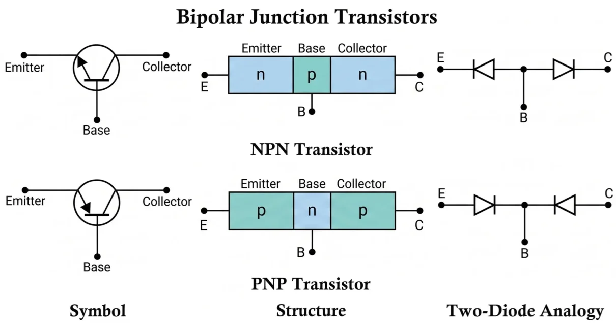
The Bipolar Junction Transistor (BJT) is one of the most important semiconductor devices used in modern electronic circuits. It consists of three semiconductor regions known as the emitter, base, and collector, which are formed by joining either two n-type regions with one p-type region or two p-type regions with one n-type region. Depending on this arrangement, a transistor is classified as either an NPN transistor or a PNP transistor.
Although both transistor types perform similar functions such as amplification and switching, their internal semiconductor arrangement and current flow directions are different. Understanding the physical structure of NPN and PNP transistors is essential for learning transistor operation, biasing, characteristics, and circuit design.
Related Articles:
- Bipolar Junction Transistor (BJT): Construction and Working
- MOSFET: Metal Oxide Semiconductor Field Effect Transistor
- JFET Junction Field Effect Transistors Working and Applications
- IGBT Full Form, Symbol, Construction, Working and Applications
- UJT Unijunction Transistor Symbol, Construction & Working
- Difference Between Photodiode, Phototransistor and Photoresistor
- Types of Transistors: Classification (BJT, JFET, MOSFET & IGBT)
Structure of NPN and PNP Bipolar Junction Transistors
A Bipolar Junction Transistor is manufactured by carefully joining three layers of semiconductor material. These layers form two PN junctions and three distinct regions Emitter (E), Base (B) and Collector (C). The arrangement of these regions determines whether the transistor is an NPN or PNP transistor.

Unlike a simple PN junction diode, a BJT contains two closely spaced junctions that allow charge carriers to move from the emitter to the collector through the thin base region. This unique structure enables the transistor to amplify electrical signals and operate as an electronic switch.
Structure of NPN Bipolar Junction Transistor
An NPN transistor is formed by placing a thin P-type semiconductor layer between two N-type semiconductor layers.
The three regions are arranged as:
N (Emitter) → P (Base) → N (Collector)
In this structure:
- The emitter is made of heavily doped N-type material.
- The base is a very thin and lightly doped P-type region.
- The collector is an N-type region having a larger physical area than the emitter.
When properly biased, electrons are injected from the emitter into the base. Since the base is extremely thin and lightly doped, most of these electrons pass through it and are collected by the collector, resulting in efficient transistor operation.
Structure of PNP Bipolar Junction Transistor
A PNP transistor is constructed by sandwiching a thin N-type semiconductor layer between two P-type semiconductor layers.
The arrangement becomes:
P (Emitter) → N (Base) → P (Collector)
Its structural characteristics are similar to those of an NPN transistor except that the semiconductor polarities are reversed.
- The emitter is heavily doped P-type material.
- The base is a thin, lightly doped N-type layer.
- The collector is a P-type region with a comparatively larger area.
During operation, holes act as the majority charge carriers. They move from the emitter towards the collector through the thin base region.
Emitter, Base and Collector Regions
Each region of a transistor is specially designed to perform a specific function. Their size, doping concentration, and position are carefully selected during manufacturing.

Emitter (E)
The emitter is responsible for supplying the majority charge carriers into the base region.
- Located at one end of the transistor.
- Heavily doped to inject a large number of charge carriers.
- Provides electrons in NPN transistors and holes in PNP transistors.
The high doping concentration improves emitter efficiency and allows maximum carrier injection into the base.
Base (B)
The base is the central region of the transistor and plays the most critical role in controlling transistor operation.
- Extremely thin compared to the emitter and collector.
- Very lightly doped.
- Controls the movement of charge carriers between emitter and collector.
Because the base is thin and lightly doped, only a very small number of charge carriers recombine inside it. As a result, almost all injected carriers continue toward the collector, enabling current amplification.
Collector (C)
The collector collects the charge carriers that travel through the base.
- Moderately to heavily doped.
- Physically larger than the emitter.
- Designed to withstand higher voltage and dissipate more heat.
The collector region handles most of the transistor’s power dissipation during operation, making its larger size essential for reliable performance.
Doping in NPN and PNP Transistors
Doping is the process of adding controlled impurities to a pure semiconductor material such as silicon or germanium to modify its electrical conductivity.
Each transistor region is doped differently to achieve efficient operation.
| Region | Doping Level | Purpose |
|---|---|---|
| Emitter | Heavily Doped | Inject maximum charge carriers |
| Base | Lightly Doped | Minimize recombination of carriers |
| Collector | Moderately Doped | Collect carriers and withstand higher voltage |
This carefully controlled doping profile is one of the main reasons why a transistor can amplify signals efficiently.
Why is the Base Thin and Lightly Doped?
The base is intentionally made extremely thin and lightly doped to reduce the recombination of charge carriers.
When carriers enter the base from the emitter, only a small percentage recombines with the opposite carriers present in the base. The remaining carriers successfully pass through the base and reach the collector.
This design allows a very small base current to control a much larger collector current, which is the fundamental principle behind transistor amplification.
Why is the Emitter Heavily Doped?
The emitter must inject as many majority charge carriers as possible into the base. For this reason, it is heavily doped compared to the collector.
A higher doping concentration increases the availability of free electrons in an NPN transistor or free holes in a PNP transistor, improving emitter injection efficiency and overall transistor gain.
Why is the Collector Larger than the Emitter?
The collector region is designed with a larger physical area than the emitter for several important reasons.
- It handles higher collector voltage.
- It carries most of the transistor current.
- It dissipates more power during operation.
- Its larger surface area improves heat dissipation and increases device reliability.
Although the collector is slightly less heavily doped than the emitter, its larger size allows it to safely collect charge carriers under high-power operating conditions.
PN Junctions in a Bipolar Junction Transistor
A transistor contains two PN junctions formed by the three semiconductor regions.
Emitter-Base Junction (JE): This junction exists between the emitter and the base. During normal transistor operation, it is forward biased, allowing majority charge carriers to enter the base region.
Collector-Base Junction (JC): This junction exists between the collector and the base. Under active operating conditions, it is reverse biased. The electric field created by this reverse bias attracts charge carriers from the base into the collector, completing transistor action.
The combined operation of these two junctions allows a transistor to amplify signals with high efficiency.
Diode Equivalent Structure of a Transistor
A Bipolar Junction Transistor consists of two PN junctions, so it can be represented structurally as two diodes connected back-to-back.

This equivalent representation is useful for understanding the presence of two PN junctions:
- Emitter-Base junction
- Collector-Base junction
However, this representation is only for understanding the internal construction. It does not accurately represent the electrical operation of a transistor.
Why Two Back-to-Back Diodes Cannot Replace a Transistor
Although a transistor appears similar to two PN junction diodes connected together, two ordinary diodes cannot function as a Bipolar Junction Transistor.
The main reasons are:
- Different Doping Profile: A transistor requires carefully controlled doping levels in the emitter, base, and collector regions. Ordinary diodes do not satisfy these requirements.
- Thin Common Base Region: In a transistor, both PN junctions share the same thin base region. This common region allows injected charge carriers to diffuse directly from the emitter to the collector. Two separate diodes do not share a common semiconductor layer, so this carrier transport mechanism cannot occur.
- Carrier Diffusion: In an operating transistor, almost the entire emitter current reaches the collector through carrier diffusion. In contrast, back-to-back diodes behave as two independent devices, where one diode remains reverse biased, allowing only a very small reverse saturation current to flow.
- No Current Amplification: Because the required carrier transport does not occur between two separate diodes, they cannot provide the current amplification or switching action of a transistor.
Comparison of NPN and PNP Transistor Structure
| Feature | NPN Transistor | PNP Transistor |
|---|---|---|
| Semiconductor Layers | N-P-N | P-N-P |
| Base Material | P-Type | N-Type |
| Emitter Material | N-Type | P-Type |
| Collector Material | N-Type | P-Type |
| Majority Charge Carrier | Electrons | Holes |
| Number of PN Junctions | Two | |
| Base Thickness | Very Thin and Lightly Doped | |
| Collector Area | Larger than Emitter | |
| Examples | 2N2222, BC547, BC548 | 2N2907, BC557, BC558 |
Features of BJT Structure
- A BJT consists of three semiconductor regions: emitter, base, and collector.
- It contains two PN junctions.
- The emitter is heavily doped for efficient carrier injection.
- The base is extremely thin and lightly doped to minimize carrier recombination.
- The collector has a larger area for better heat dissipation and higher power handling.
- The transistor structure enables efficient current amplification and switching.
- Two ordinary back-to-back diodes cannot replace a transistor because they lack the required common base region and doping profile.
Conclusion
The Structure of NPN and PNP Bipolar Junction Transistors is carefully engineered to achieve efficient amplification and switching. Although both transistor types have similar construction, the arrangement of semiconductor layers and the direction of charge carrier movement are opposite. The heavily doped emitter, thin lightly doped base, and larger collector work together to provide high current gain and reliable performance. A thorough understanding of the transistor’s physical structure forms the foundation for learning transistor operation, biasing methods, characteristics, and practical electronic circuit design.
Bipolar Junction Transistor (BJT): Construction, Working, Types, Characteristics and Applications
IGBT Full Form, Symbol, Construction, Working and Applications
JFET Junction Field Effect Transistors Working and Applications
UJT Unijunction Transistor Symbol, Construction, Working & Applications
Difference Between Photodiode, Phototransistor and Photoresistor
Unbiased PN Junction: Depletion Region and Barrier Potential

