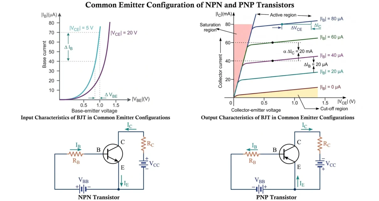
The Common Emitter (CE) configuration is one of the three basic BJT (Bipolar Junction Transistor) configurations, along with the Common Base (CB) and Common Collector (CC) configurations. It is the most widely used because it provides high current gain, high voltage gain, and high power gain, making it ideal for amplifiers, switching circuits, oscillators, and many analog and digital applications.
In the CE configuration, the emitter is common to both the input and output circuits. The input signal is applied between the base and emitter, while the output is taken between the collector and emitter.
The transistor’s operation is analyzed using its input and output characteristic curves:
- Input Characteristics: Relationship between base-emitter voltage (VBE) and base current (IB) at a constant collector-emitter voltage (VCE).
- Output Characteristics: Relationship between collector-emitter voltage (VCE) and collector current (IC) for different values of base current (IB).
These characteristics help determine the active, saturation, and cut-off regions, along with current gain (β), input resistance, output resistance, voltage gain, and the Q-point for stable amplifier operation.
The CE configuration can be implemented with both NPN and PNP transistors. Although their current directions and voltage polarities differ, both operate on the same principle: the base-emitter junction is forward biased and the collector-base junction is reverse biased, allowing a small base current to control a much larger collector current.
Compared with the CB and CC configurations, the Common Emitter configuration provides the highest overall power gain. It offers moderate input resistance, high output resistance, and a 180° phase shift between the input and output, making it the preferred choice for audio and voltage amplifiers, transistor switches, sensor interfaces, communication circuits, and general-purpose electronic designs.
Related Articles:
- Biasing and Operation of NPN and PNP Transistors
- Bipolar Junction Transistor (BJT): Construction and Working
- MOSFET: Metal Oxide Semiconductor Field Effect Transistor
- JFET Junction Field Effect Transistors Working and Applications
- IGBT Full Form, Symbol, Construction, Working and Applications
- UJT Unijunction Transistor Symbol, Construction & Working
- Types of Transistors: Classification (BJT, JFET, MOSFET & IGBT)
In the following sections, we will study the Common Emitter Configuration of NPN and PNP Transistors, including its circuit diagrams, current relationships, current gain (β), characteristics, operating regions, leakage currents, advantages, disadvantages, applications, and design considerations.
Common Emitter Configuration of NPN and PNP Transistors
In the Common Emitter (CE) configuration, the emitter terminal of the Bipolar Junction Transistor (BJT) is common to both the input and output circuits. The input signal is applied between the base and emitter, while the output is taken between the collector and emitter. Since the emitter acts as the common reference terminal for both circuits, this transistor connection is known as the Common Emitter Configuration.
Common Emitter Configuration of NPN and PNP Transistors
The Common Emitter configuration can be implemented using both NPN and PNP transistors. Although the polarity of the supply voltages and the direction of current flow differ between these two transistor types, their operating principle remains the same. In both cases, the transistor functions as an amplifier when the base-emitter junction (JE) is forward biased and the collector-base junction (JC) is reverse biased.

Common Emitter Configuration of an NPN Transistor
In an NPN transistor connected in the Common Emitter configuration, the emitter terminal is generally connected to the ground or the negative supply and acts as the common terminal. The input signal is applied between the base and emitter, while the output is obtained between the collector and emitter.
- The base-emitter junction is forward biased by making the base positive with respect to the emitter.
- The collector-base junction is reverse biased by making the collector more positive than the base.
- A small base current (IB) flows into the transistor through the forward-biased base-emitter junction.
- The majority charge carriers (electrons) are injected from the emitter into the thin base region.
- Most of these electrons pass through the thin, lightly doped base without recombination and are attracted to the collector by the reverse-biased collector-base junction.
- Only a small number of electrons recombine with holes in the base region, producing the base current.
- As a result, a very small change in the base current controls a much larger collector current, giving the Common Emitter configuration a high current gain (β).
Common Emitter Configuration of a PNP Transistor
The PNP transistor is connected in the same manner as the NPN transistor, except that all voltage polarities and current directions are reversed. The emitter remains the common terminal, the input is applied between the base and emitter, and the output is taken between the collector and emitter.
- The base-emitter junction is forward biased by making the base negative with respect to the emitter.
- The collector-base junction is reverse biased by making the collector more negative than the base.
- The majority charge carriers (holes) are injected from the emitter into the base region.
- Most of these holes cross the thin base with very little recombination and are collected by the collector.
- Only a small fraction of holes recombine within the base, producing a small base current.
- Consequently, the collector current is controlled by the base current, just as in an NPN transistor, providing a high current amplification factor.
Terminal Connections in Common Emitter Configuration
| Parameter | NPN Transistor | PNP Transistor |
|---|---|---|
| Common Terminal | Emitter | Emitter |
| Input Applied Between | Base and Emitter | Base and Emitter |
| Output Taken Between | Collector and Emitter | Collector and Emitter |
| Base-Emitter Junction | Forward Biased | Forward Biased |
| Collector-Base Junction | Reverse Biased | Reverse Biased |
| Majority Charge Carriers | Electrons | Holes |
| Collector Voltage with Respect to Emitter | Positive | Negative |
| Base Voltage with Respect to Emitter | Positive | Negative |
Characteristics of Common Emitter Configuration
The Common Emitter configuration possesses several electrical characteristics that make it the most popular transistor configuration for amplification and switching applications. Its ability to provide both current and voltage amplification results in the highest overall power gain among the three transistor configurations.
- Provides moderate input resistance, typically ranging from 1 kΩ to 10 kΩ, making it suitable for most signal sources.
- Offers high output resistance, generally ranging from 10 kΩ to 50 kΩ, depending on the transistor and operating conditions.
- Has a high current gain (β), typically between 20 and 500, with values of 50 to 200 being common for general-purpose BJTs.
- Provides substantial voltage gain as well as the highest power gain among the CB, CE, and CC configurations.
- Introduces a 180° phase shift between the input and output voltages, meaning the output signal is inverted with respect to the input.
- Can be used both as a linear amplifier in the active region and as an electronic switch by operating between the cut-off and saturation regions.
- Suitable for a wide range of applications, including audio amplifiers, voltage amplifiers, sensor interfaces, oscillator circuits, transistor switches, digital logic circuits, and communication systems.
A thorough understanding of the Common Emitter configuration is essential before studying its current relationships and characteristic curves. In the following sections, we will examine the current relations, current gain (β), leakage currents, input characteristics, output characteristics, operating regions, and practical performance of the Common Emitter configuration in detail.
Current Relations in Common Emitter (CE) Configuration
The current relationships in the Common Emitter (CE) configuration describe the mathematical relationship between the base current (IB), collector current (IC), and emitter current (IE). In this configuration, the emitter terminal is common to both the input and output circuits. The input current is the base current, while the output current is the collector current.

When the transistor operates in the active region, the base-emitter junction is forward biased and the collector-base junction is reverse biased. A small base current controls the movement of a much larger number of charge carriers from the emitter to the collector. As a result, a slight change in the base current produces a significant change in the collector current, which is the fundamental principle behind transistor amplification.
Basic Current Relationship
Like every Bipolar Junction Transistor (BJT), the Common Emitter configuration follows the fundamental current equation:
IE = IC + IB
This equation indicates that the emitter current is divided into two components:
- Collector Current (IC) – The major portion of the emitter current that reaches the collector.
- Base Current (IB) – A small portion of the emitter current that recombines within the base region.
Since the base is very thin and lightly doped, only a small fraction of the injected charge carriers recombine in the base. Therefore, the collector current is much larger than the base current.
Collector Current Equation
The collector current in the Common Emitter configuration consists of two components:
- Injected Collector Current (IC(INJ)) – Produced by the majority charge carriers injected from the emitter that successfully reach the collector.
- Collector-Base Leakage Current (ICBO) – A very small reverse leakage current flowing through the reverse-biased collector-base junction due to minority charge carriers.
Therefore, the collector current is expressed as:
IC = IC(INJ) + ICBO
Since the injected collector current is directly proportional to the base current, the practical collector current in the Common Emitter configuration becomes:
IC = βIB + (1 + β)ICBO
Under normal operating conditions, the leakage current ICBO is extremely small compared to the collector current and is therefore neglected. The collector current equation simplifies to:
IC ≈ βIB
However, at elevated temperatures, the leakage current increases significantly and must be considered in precision amplifier and biasing circuit design.
Current Gain (βDC) in Common Emitter Configuration
The DC current gain of a transistor in the Common Emitter configuration is represented by the Greek letter β (beta). It is also known as the Common Emitter Current Gain or the Current Amplification Factor. It represents how many times the collector current is greater than the base current.
It is defined as:
βDC = β = IC / IB
Rearranging the equation gives:
IC = βIB
Unlike the Common Base current gain (α), which is always less than one, the value of β is much greater than unity. For most practical silicon transistors, its value typically lies within the range:
20 ≤ β ≤ 500
General-purpose BJTs commonly have a DC current gain between 50 and 200, depending on the transistor type and manufacturing process.
Relationship Between α and β
The current gains α (Common Base) and β (Common Emitter) are closely related because both describe the same transistor using different input and output currents.
Starting with the basic transistor equation:
IE = IC + IB
Since:
α = IC / IE
and
β = IC / IB
the relationship between them becomes:
β = α / (1 – α)
Similarly,
α = β / (1 + β)
These equations are widely used to convert the current gain from one transistor configuration to another.
Leakage Current in Common Emitter Configuration (ICEO)
When the base terminal is left open (IB = 0), a small collector current still flows because of the reverse leakage current through the collector-base junction. In the Common Emitter configuration, this leakage current is known as the Collector-Emitter Leakage Current (ICEO).
It is related to the Common Base leakage current by:
ICEO = (1 + β)ICBO
Since β is usually quite large, even a very small value of ICBO can produce a noticeable value of ICEO. This leakage current increases rapidly with temperature and is an important factor in transistor bias stability.
| Parameter | Formula |
|---|---|
| Emitter Current | IE = IC + IB |
| Current Gain | β = IC / IB |
| Collector Current | IC = βIB |
| Collector Current (Including Leakage) | IC = βIB + (1 + β)ICBO |
| Leakage Current | ICEO = (1 + β)ICBO |
| Relationship Between α and β | β = α / (1 – α) |
| Relationship Between β and α | α = β / (1 + β) |
Numerical Example
Given:
- Base Current, IB = 50 µA
- Current Gain, β = 100
- Collector-Base Leakage Current, ICBO = 1 µA
Collector Current:
IC = βIB + (1 + β)ICBO
= (100 × 50 µA) + (101 × 1 µA)
= 5000 µA + 101 µA
IC = 5101 µA = 5.101 mA
Emitter Current:
IE = IC + IB
= 5.101 mA + 0.05 mA
IE = 5.151 mA
- The emitter current is always the sum of the collector current and the base current.
- A very small base current controls a much larger collector current, enabling current amplification.
- The DC current gain (β) of the Common Emitter configuration is much greater than unity and is the primary reason for its widespread use in amplifier circuits.
- The collector-emitter leakage current (ICEO) is considerably larger than the collector-base leakage current (ICBO) because it is multiplied by the transistor’s current gain.
- Both leakage currents increase with temperature and must be considered in transistor biasing and thermal stability analysis.
- The current relationships discussed above form the foundation for understanding the input characteristics, output characteristics, gain analysis, and practical design of Common Emitter transistor circuits.
Input Characteristics (Base Curves) of Common Emitter Configuration
The input characteristics of a transistor in the Common Emitter (CE) configuration describe the relationship between the base-emitter voltage (VBE) and the corresponding base current (IB) while keeping the collector-emitter voltage (VCE) constant. These characteristics are commonly known as the base characteristics because they represent the input behavior of the transistor through its base terminal.
Since the base-emitter junction is forward biased during normal transistor operation, the input characteristic closely resembles the forward V-I characteristic of a PN junction diode. Initially, the base current is almost zero, but once the applied base-emitter voltage exceeds the cut-in voltage, the base current increases rapidly with a small increase in voltage.

To obtain the input characteristics experimentally, the collector-emitter voltage (VCE) is maintained at a constant value while the base-emitter voltage (VBE) is gradually increased. The corresponding base current (IB) is measured and plotted. This procedure is repeated for different values of VCE, resulting in a family of input characteristic curves.
Input Characteristic Curve
The input characteristic graph is plotted as follows:
- X-axis: Base-Emitter Voltage (VBE)
- Y-axis: Base Current (IB)
- Collector-Emitter Voltage (VCE) is kept constant for each characteristic curve.
Initially, when the applied base-emitter voltage is below the cut-in voltage, only a negligible base current flows because the PN junction barrier has not yet been overcome. Once the applied voltage exceeds the junction’s threshold voltage, the base current increases exponentially, producing the familiar diode-like input characteristic.
Input Resistance
The dynamic input resistance of the Common Emitter configuration is defined as the ratio of the change in base-emitter voltage to the corresponding change in base current while maintaining a constant collector-emitter voltage.
Input Resistance (ri) = ΔVBE / ΔIB
where,
- ΔVBE = Change in base-emitter voltage
- ΔIB = Corresponding change in base current
- VCE = Constant collector-emitter voltage
Although the input characteristic resembles that of a forward-biased diode, the input resistance of the Common Emitter configuration is considerably higher than that of the Common Base configuration because the input current is the much smaller base current rather than the emitter current. In practical transistor circuits, the input resistance typically ranges from approximately 1 kΩ to 10 kΩ, depending on the transistor type and operating conditions.
Effect of Cut-In Voltage
The base-emitter junction behaves exactly like a forward-biased PN junction diode. Therefore, the base current remains extremely small until the applied voltage exceeds the transistor’s cut-in (threshold) voltage.
- For a Silicon (Si) transistor, the cut-in voltage is approximately 0.7 V.
- For a Germanium (Ge) transistor, the cut-in voltage is approximately 0.3 V.
Once this voltage is reached, even a slight increase in VBE causes a large increase in IB due to the exponential conduction characteristics of the PN junction.
Effect of Collector-Emitter Voltage (VCE)
An important feature of the Common Emitter input characteristics is that the base current decreases slightly as the collector-emitter voltage (VCE) increases, even when the base-emitter voltage remains constant.
This behavior is caused by the Early Effect (Base Width Modulation). As the reverse bias across the collector-base junction increases, its depletion region widens into the base region, effectively reducing the base width. Since the base becomes thinner, fewer charge carriers recombine inside it, and more carriers are swept into the collector.
As a result, for the same value of VBE, the transistor requires a slightly smaller base current to maintain conduction. Consequently, the input characteristic curves shift slightly downward as VCE increases.
Voltage Polarities in NPN and PNP Transistors
The voltage polarities in the Common Emitter configuration depend on whether the transistor is an NPN or PNP device. Although the operating principle remains identical, the voltage polarities are opposite.
| Parameter | NPN Transistor | PNP Transistor |
|---|---|---|
| Base-Emitter Voltage (VBE) | Positive | Negative |
| Collector-Emitter Voltage (VCE) | Positive | Negative |
| Base-Emitter Junction | Forward Biased | Forward Biased |
| Collector-Base Junction | Reverse Biased | Reverse Biased |
Observations from the Input Characteristics
- The input characteristic closely resembles the forward V-I characteristic of a PN junction diode because the base-emitter junction is forward biased.
- The base current remains almost zero until the cut-in voltage is reached.
- Beyond the cut-in voltage, a very small increase in base-emitter voltage produces a rapid increase in base current.
- The Common Emitter configuration has a moderate input resistance, which is significantly higher than that of the Common Base configuration because the input current is the comparatively small base current.
- As the collector-emitter voltage increases, the base current decreases slightly for the same value of base-emitter voltage due to the Early Effect (Base Width Modulation).
- The input characteristics are used to determine the transistor’s dynamic input resistance and to select an appropriate operating point (Q-point) for amplifier design.
- The shape of the input characteristic confirms that the base-emitter junction behaves like a forward-biased semiconductor diode.
The input characteristics clearly demonstrate that the Common Emitter configuration provides a moderate input impedance, making it suitable for interfacing with a wide variety of signal sources. Combined with its high current gain and voltage gain, this characteristic is one of the primary reasons why the Common Emitter configuration is the most widely used transistor configuration in amplifier and switching circuits.
Output Characteristics (Collector Curves) of Common Emitter Configuration
The output characteristics of a transistor in the Common Emitter (CE) configuration describe the relationship between the collector current (IC) and the collector-emitter voltage (VCE) for different fixed values of base current (IB). These characteristics are also known as the collector characteristics because they represent the output behavior of the transistor through its collector terminal.
The output characteristics are among the most important graphs used in transistor analysis because they illustrate how the transistor operates under different biasing conditions. They help identify the cut-off, active, and saturation regions, determine the transistor’s output resistance, estimate the current gain (β), and select the proper operating point (Q-point) for amplifier and switching applications.

To obtain the output characteristics experimentally, the base current (IB) is maintained at a constant value while the collector-emitter voltage (VCE) is gradually increased. The corresponding collector current (IC) is measured and plotted. The experiment is repeated for different values of base current, producing a family of collector characteristic curves.
Output Characteristic Curve
The output characteristic graph is plotted as follows:
- X-axis: Collector-Emitter Voltage (VCE)
- Y-axis: Collector Current (IC)
- Base Current (IB) is kept constant for each characteristic curve.
Each curve corresponds to a particular value of base current. As the base current increases, the collector current also increases proportionally, demonstrating the current amplification capability of the Common Emitter configuration.
Output Resistance
The dynamic output resistance of the Common Emitter configuration is defined as the ratio of the change in collector-emitter voltage to the corresponding change in collector current while maintaining a constant base current.
Output Resistance (ro) = ΔVCE / ΔIC
where,
- ΔVCE = Change in collector-emitter voltage
- ΔIC = Corresponding change in collector current
- IB = Constant base current
In the active region, increasing the collector-emitter voltage causes only a very small increase in collector current. Therefore, the output resistance of the Common Emitter configuration is relatively high, making it suitable for voltage amplification.
Determination of Current Gain (β)
The DC current gain of the transistor can be determined directly from the output characteristics by taking the ratio of the collector current to the corresponding base current at any operating point.
βDC = IC / IB
Since the collector current is controlled by the base current, increasing IB shifts the operating point upward to a higher collector current. This property enables the Common Emitter configuration to provide substantial current and power amplification.
Operating Regions of Common Emitter Configuration
The output characteristics of the Common Emitter configuration are divided into three important operating regions:
Active Region
The active region is the normal operating region for transistor amplifiers. In this region:
- The base-emitter junction is forward biased.
- The collector-base junction is reverse biased.
- The collector current is approximately proportional to the base current.
- A small increase in base current produces a much larger increase in collector current.
- The transistor operates as a linear amplifier with high current, voltage, and power gain.
Although the collector current ideally remains constant for a fixed base current, a slight increase is observed with increasing VCE because of the Early Effect (Base Width Modulation).
Saturation Region
The saturation region occurs when both transistor junctions become forward biased.
- The base-emitter junction is forward biased.
- The collector-base junction is also forward biased.
- The collector current no longer increases proportionally with the base current.
- The transistor behaves like a closed switch (ON state) with very low collector-emitter voltage.
The collector-emitter saturation voltage is represented by:
VCE(sat) ≈ 0.1 V to 0.3 V
In practical silicon transistors, the saturation voltage is commonly around 0.2 V, although it varies with transistor type and collector current.
Cut-Off Region
The cut-off region is obtained when the base current becomes zero or insufficient to forward bias the base-emitter junction.
- Both the base-emitter and collector-base junctions are reverse biased.
- The collector current becomes nearly zero except for a very small leakage current.
- The transistor behaves like an open switch (OFF state).
- This operating region is widely used in digital switching circuits.
Voltage Polarities in NPN and PNP Transistors
The voltage polarities of the Common Emitter output characteristics depend on whether the transistor is an NPN or PNP device.
| Parameter | NPN Transistor | PNP Transistor |
|---|---|---|
| Collector-Emitter Voltage (VCE) | Positive | Negative |
| Collector Current (IC) | Flows from Collector to Emitter | Flows from Emitter to Collector |
| Base Current (IB) | Flows into Base | Flows out of Base |
| Amplifier Operating Region | Active Region | Active Region |
Observations from the Output Characteristics
- The output characteristics show the relationship between collector current (IC) and collector-emitter voltage (VCE) for different fixed values of base current (IB).
- The collector current is primarily controlled by the base current rather than the collector-emitter voltage.
- For a fixed base current, increasing VCE causes only a slight increase in collector current due to the Early Effect.
- The dynamic output resistance of the Common Emitter configuration is relatively high because the change in collector current is very small compared to the change in collector-emitter voltage.
- The output characteristics clearly identify the cut-off, active, and saturation regions, which are essential for amplifier and switching circuit design.
- The current gain (β) can be determined directly from the ratio of collector current to base current at any operating point.
- The output characteristics are widely used for selecting the optimum Q-point, ensuring stable transistor operation with minimum distortion and maximum signal swing.
The output characteristics demonstrate why the Common Emitter configuration is the most widely used transistor configuration. Its ability to provide high current gain, substantial voltage gain, and clear operating regions makes it ideal for analog amplifiers, digital switches, oscillator circuits, communication systems, and a wide range of electronic applications.
Early Effect (Base Width Modulation) in Common Emitter Configuration
The Early Effect, also known as Base Width Modulation, is one of the most important non-ideal characteristics of a Bipolar Junction Transistor (BJT). In the Common Emitter (CE) configuration, it occurs when the collector-emitter voltage (VCE) increases while the transistor operates in the active region. As the collector voltage increases, the reverse bias across the collector-base junction also increases, causing its depletion region to expand into the thin base region. This effectively reduces the width of the neutral base, influencing the movement of charge carriers and slightly increasing the collector current.
The Early Effect was first explained by the American physicist James M. Early, after whom the phenomenon is named. Although the physical reduction in base width is extremely small, its electrical effects become significant in high-gain amplifier circuits, precision analog systems, current mirrors, differential amplifiers, and integrated circuits.
Why Does the Early Effect Occur?
During normal operation of a transistor in the Common Emitter configuration:
- The base-emitter junction (JE) is forward biased.
- The collector-base junction (JC) is reverse biased.
When the collector-emitter voltage (VCE) is increased, the reverse bias across the collector-base junction also increases. As a result, the depletion region surrounding this junction widens. Since the base is intentionally made very thin and lightly doped, most of the depletion region expands into the base rather than the collector.
This expansion reduces the effective width of the neutral base, a phenomenon known as Base Width Modulation or the Early Effect.
Working of the Early Effect
Under normal transistor operation, majority charge carriers are injected from the emitter into the base region through the forward-biased base-emitter junction. While passing through the thin base, a small number of carriers recombine with the majority carriers present in the base, producing the base current (IB). The remaining carriers are swept into the collector by the reverse-biased collector-base junction, producing the collector current (IC).
When the effective base width decreases because of an increase in VCE:
- The distance travelled by charge carriers through the base becomes shorter.
- The probability of carrier recombination inside the base decreases.
- A larger number of injected carriers successfully reach the collector.
- The collector current (IC) increases slightly even though the base current (IB) remains nearly constant.
- The transistor’s current gain (β) increases slightly because more collector current is produced for the same base current.
This explains why the collector characteristic curves of the Common Emitter configuration are not perfectly horizontal in the active region. Instead, they exhibit a slight upward slope as the collector-emitter voltage increases.
Effects of Base Width Modulation
The reduction in effective base width produces several important effects on transistor performance.
Increase in Collector Current
As the neutral base becomes thinner, fewer charge carriers recombine within the base region. Consequently, a larger percentage of carriers reach the collector, causing the collector current to increase slightly even though the base current remains almost unchanged.
Increase in Current Gain (β)
Since the collector current increases while the base current changes very little, the Common Emitter current gain increases slightly.
β = IC / IB
Although the increase is relatively small, it becomes important in precision analog circuits where stable transistor gain is required.
Finite Output Resistance
Ideally, the collector current in the active region should remain completely independent of the collector-emitter voltage. However, due to the Early Effect, the collector current increases slightly as VCE increases.
Consequently, the transistor exhibits a large but finite output resistance instead of an ideal infinite output resistance. This finite output resistance influences amplifier gain, current mirrors, and active load circuits.
Output Resistance (ro) = ΔVCE / ΔIC
Improved Carrier Transport Efficiency
A thinner base allows injected charge carriers to cross the base more efficiently with reduced recombination losses. This slightly improves the transistor’s carrier transport efficiency and contributes to better current transfer from the emitter to the collector.
Early Voltage (VA)
The magnitude of the Early Effect is represented by a parameter known as the Early Voltage (VA). If the nearly straight portions of the Common Emitter output characteristic curves are extended backward, they intersect the voltage axis at a negative value known as the Early voltage.
A transistor with a larger Early voltage experiences less base width modulation and therefore exhibits:
- Better collector current stability.
- Higher output resistance.
- Greater voltage gain.
- Improved linearity.
- Lower signal distortion in amplifier circuits.
For practical silicon BJTs, the Early voltage typically ranges from approximately 20 V to over 200 V, depending on the transistor structure and manufacturing process.
Advantages of the Early Effect
- Improves charge carrier collection efficiency.
- Slightly increases the Common Emitter current gain (β).
- Enhances voltage gain in transistor amplifier circuits.
- Improves the transport efficiency of carriers through the base region.
- Contributes to better performance in high-gain amplifier stages.
Disadvantages of the Early Effect
- The collector current becomes dependent on the collector-emitter voltage instead of remaining perfectly constant.
- Reduces the accuracy of transistor biasing in precision analog circuits.
- Introduces non-linearity and harmonic distortion in amplifier circuits.
- Causes transistor parameters such as current gain and output resistance to vary with operating voltage.
- Produces finite output resistance, limiting the ideal constant-current behavior of the transistor.
Important Observation
- The Early Effect is also known as Base Width Modulation.
- It occurs because increasing the collector-emitter voltage (VCE) increases the reverse bias across the collector-base junction.
- The expanded depletion region reduces the effective width of the transistor’s neutral base.
- A thinner base reduces carrier recombination, allowing more charge carriers to reach the collector.
- As a result, the collector current increases slightly even when the base current remains nearly constant.
- The Common Emitter current gain (β) increases slightly because more collector current is obtained for the same base current.
- The slight upward slope observed in the active region of the Common Emitter output characteristics is a direct consequence of the Early Effect.
- The Early Effect plays an important role in the design of voltage amplifiers, current mirrors, differential amplifiers, active loads, and integrated circuits.
A clear understanding of the Early Effect in the Common Emitter configuration is essential for accurately analyzing transistor behavior and designing stable, high-performance amplifier circuits. Although it introduces non-ideal characteristics into practical BJTs, engineers take the Early Effect into account to optimize gain, improve bias stability, reduce distortion, and achieve reliable performance in modern electronic systems.
Advantages of Common Emitter Configuration
- Provides high current gain (β), allowing a small base current to control a much larger collector current.
- Offers high voltage gain, making it suitable for voltage amplification.
- Delivers the highest overall power gain among the CB, CE, and CC transistor configurations.
- Has moderate input resistance, making it compatible with most signal sources.
- Provides high output resistance, which is desirable for amplifier circuits.
- Can operate as both an amplifier (active region) and an electronic switch (cut-off and saturation regions).
- Requires simple biasing and circuit design, making implementation straightforward.
- Widely available and economical for general-purpose analog and digital circuits.
- Suitable for a broad range of low- and medium-frequency applications.
Disadvantages of Common Emitter Configuration
- Produces a 180° phase shift between the input and output signals.
- Performance is affected by temperature variations and leakage currents.
- The Early Effect (Base Width Modulation) introduces finite output resistance and slight non-linearity.
- Requires proper bias stabilization to maintain a stable operating point (Q-point).
- Voltage gain and current gain may vary with transistor parameters and operating conditions.
- Not suitable for very high-frequency applications due to internal capacitances and the Miller effect.
- Can introduce distortion if the transistor operates outside the active region.
Applications of Common Emitter Configuration
- Audio amplifiers for amplifying low-level audio signals.
- Voltage amplifiers in analog electronic circuits.
- Transistor switching circuits for digital and power control applications.
- Oscillator circuits used in signal generation.
- RF and communication circuits requiring moderate-frequency amplification.
- Sensor signal conditioning and interface circuits.
- Microcontroller and digital logic interfaces.
- Preamplifier and driver stages in multistage amplifier systems.
- Power amplifier driver circuits.
- General-purpose analog electronic circuits requiring high gain and stable amplification.
Conclusion
The Common Emitter (CE) configuration is the most widely used BJT configuration because it provides high current gain, high voltage gain, and high-power gain. In this configuration, the emitter is common to both the input and output circuits, with the input applied between the base-emitter and the output taken from the collector-emitter. This makes it ideal for both amplification and switching applications.
The CE configuration operates on the relationship between the base, collector, and emitter currents, where the current gain (β) allows a small base current to control a much larger collector current. Its input and output characteristics help determine important parameters such as current gain, input resistance, output resistance, and the Q-point.
An important non-ideal effect is the Early Effect (Base Width Modulation), where increasing collector-emitter voltage slightly increases collector current and reduces output resistance. Understanding this effect is important for accurate amplifier design.
Compared with Common Base (CB) and Common Collector (CC) configurations, the Common Emitter configuration offers the best overall amplification performance. It is widely used in audio amplifiers, voltage amplifiers, transistor switches, oscillators, communication systems, sensor interfaces, and microcontroller circuits.
Mastering the Common Emitter configuration of NPN and PNP transistors provides a strong foundation for advanced topics such as transistor biasing, multistage amplifiers, differential amplifiers, power amplifiers, and analog circuit design.
Frequently Asked Questions (FAQ)
1. What is a Common Emitter (CE) configuration?
The Common Emitter configuration is a BJT connection in which the emitter terminal is common to both the input and output circuits. The input signal is applied between the base and emitter, while the output is taken between the collector and emitter.
2. Why is it called the Common Emitter configuration?
It is called the Common Emitter configuration because the emitter terminal serves as the common reference point for both the input and output circuits.
3. What are the input and output terminals in a CE configuration?
The input is applied between the base and emitter, and the output is obtained between the collector and emitter.
4. What is the current gain (β) of a Common Emitter transistor?
The DC current gain is defined as:
β = IC / IB
Its value is always greater than unity and typically ranges from
20 to 500, while most general-purpose silicon
transistors have values between 50 and 200.
5. What is the relationship between emitter, collector, and base currents?
The fundamental transistor current relationship is:
IE = IC + IB
This means the emitter current is equal to the sum of the collector current and the base current.
6. Why does the Common Emitter configuration have moderate input resistance?
The base-emitter junction is forward biased and behaves like a forward-biased PN junction diode. Since the input current is the relatively small base current, the Common Emitter configuration provides a moderate input resistance, typically ranging from about 1 kΩ to 10 kΩ.
7. Why is the output resistance of the CE configuration high?
The collector-base junction remains reverse biased in the active region. Consequently, the collector current changes only slightly with collector-emitter voltage, resulting in a relatively high output resistance.
8. What are the operating regions of the Common Emitter configuration?
The transistor operates in three main regions:
- Active Region – Used for linear amplification.
- Saturation Region – Both junctions are forward biased and the transistor acts as an ON switch.
- Cut-Off Region – Both junctions are reverse biased and the transistor remains OFF.
9. Why does the Common Emitter amplifier produce a 180° phase shift?
An increase in the input base voltage increases the collector current, which causes a larger voltage drop across the collector load resistor. As a result, the collector voltage decreases, producing an output signal that is inverted by 180° with respect to the input.
10. What is the Early Effect in a Common Emitter transistor?
The Early Effect, also called Base Width Modulation, occurs when increasing the collector-emitter voltage widens the collector-base depletion region, reducing the effective base width. This slightly increases the collector current and current gain while introducing a finite output resistance.
11. What is the difference between NPN and PNP Common Emitter configurations?
Both configurations operate on the same principle. The main differences are the supply voltage polarities and the direction of current flow. In an NPN transistor, electrons are the majority carriers, whereas holes are the majority carriers in a PNP transistor.
12. What are the advantages of the Common Emitter configuration?
- High current gain (β).
- High voltage gain.
- High overall power gain.
- Moderate input resistance.
- High output resistance.
- Suitable for both amplification and switching.
- Simple biasing and circuit implementation.
13. What are the disadvantages of the Common Emitter configuration?
- Produces a 180° phase reversal between input and output.
- Performance is affected by temperature variations and leakage currents.
- The Early Effect introduces finite output resistance and slight non-linearity.
- Requires proper biasing to achieve stable operation.
14. Where is the Common Emitter configuration used?
The Common Emitter configuration is widely used in:
- Audio amplifiers
- Voltage amplifiers
- Transistor switching circuits
- Microcontroller and logic interfaces
- Oscillator circuits
- Sensor signal conditioning circuits
- Communication systems
- General-purpose analog electronic circuits
15. Why is the Common Emitter configuration the most popular BJT configuration?
The Common Emitter configuration is the most widely used because it provides the best combination of high current gain, high voltage gain, high power gain, moderate input impedance, and good overall amplification performance. These advantages make it suitable for a vast range of analog and digital electronic applications.
Bipolar Junction Transistor (BJT): Construction, Working, Types, Characteristics and Applications
IGBT Full Form, Symbol, Construction, Working and Applications
JFET Junction Field Effect Transistors Working and Applications
Types of Transistors: Classification (BJT, JFET, MOSFET & IGBT)
UJT Unijunction Transistor Symbol, Construction, Working & Applications
Unbiased PN Junction: Depletion Region and Barrier Potential

