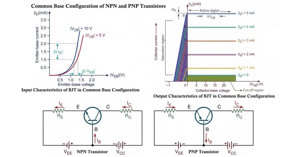
The Common Base (CB) configuration is one of the three fundamental ways of connecting a Bipolar Junction Transistor (BJT). The other two configurations are the Common Emitter (CE) and Common Collector (CC) configurations. Although the common base configuration is less frequently used than the common emitter configuration, it plays an important role in high-frequency amplifier circuits due to its excellent voltage gain, wide bandwidth, and low input impedance.
In a common base circuit, the base terminal serves as the common reference point for both the input and the output circuits. The input signal is applied between the emitter and base, while the amplified output is obtained between the collector and base. Since the base terminal is common to both sides of the circuit, this arrangement is known as the Common Base Configuration.
To completely understand the electrical behavior of a transistor, it is necessary to study the relationship between the transistor currents and voltages. These relationships are represented graphically using transistor characteristics, which describe how the transistor responds to different operating conditions. The two most important characteristics are:
- Input Characteristics – Relationship between the emitter-base voltage (VEB) and emitter current (IE).
- Output Characteristics – Relationship between the collector-base voltage (VCB) and collector current (IC).
These characteristic curves provide valuable information about the transistor’s operating regions, input and output resistances, current gain, and amplification capability. They are also useful for selecting the proper operating point (Q-point) when designing transistor amplifiers.
The common base configuration can be implemented using both NPN and PNP transistors. Although the direction of current flow and voltage polarities differ between these two transistor types, their operating principle remains the same. In both cases, the emitter-base junction is normally forward biased, while the collector-base junction is reverse biased during normal amplifier operation.
Compared to the common emitter configuration, the common base configuration offers a current gain slightly less than unity, but provides high voltage gain, very high output resistance, low input resistance, and excellent high-frequency performance. These characteristics make it particularly suitable for RF amplifiers, impedance matching networks, cascade amplifiers, and communication systems.
Related Articles:
- Biasing and Operation of NPN and PNP Transistors
- Bipolar Junction Transistor (BJT): Construction and Working
- MOSFET: Metal Oxide Semiconductor Field Effect Transistor
- JFET Junction Field Effect Transistors Working and Applications
- IGBT Full Form, Symbol, Construction, Working and Applications
- UJT Unijunction Transistor Symbol, Construction & Working
- Types of Transistors: Classification (BJT, JFET, MOSFET & IGBT)
In the following sections, we will study the Common Base Configuration of NPN and PNP Transistors in detail, including its circuit diagrams, current relationships, input and output characteristics, current gain, Early effect, operating regions, practical applications, advantages, and limitations.
Common Base Configuration of NPN and PNP Transistors
In the Common Base (CB) configuration, the base terminal of the Bipolar Junction Transistor (BJT) is common to both the input and output circuits. The input signal is applied between the emitter and base, while the output is taken between the collector and base. Since the base serves as the common reference terminal for both circuits, this transistor connection is known as the Common Base Configuration.

The common base configuration is available for both NPN and PNP transistors. Although the polarity of the supply voltages and the direction of current flow differ between these two transistor types, their operating principle remains the same. In both cases, the transistor operates as an amplifier only when the emitter-base junction (JE) is forward biased and the collector-base junction (JC) is reverse biased.
Common Base Configuration of an NPN Transistor
In an NPN transistor connected in the common base configuration, the base terminal is usually connected to the ground or a fixed reference potential. The input signal is applied between the emitter and the base, while the output is obtained from the collector with respect to the base.
- The emitter-base junction is forward biased by making the emitter negative with respect to the base.
- The collector-base junction is reverse biased by making the collector positive with respect to the base.
- The majority carriers (electrons) are injected from the emitter into the thin base region.
- Most of these electrons cross the base without recombination and are collected by the collector due to the reverse-biased collector-base junction.
- Only a small number of electrons recombine with holes in the base, resulting in a very small base current.
As a result, the collector current is almost equal to the emitter current, making the current gain of the common base configuration slightly less than unity.
Common Base Configuration of a PNP Transistor
The PNP transistor is connected in the same manner except that the voltage polarities and current directions are reversed. The base remains the common terminal, the input is applied between the emitter and base, and the output is taken between the collector and base.
- The emitter-base junction is forward biased by making the emitter positive with respect to the base.
- The collector-base junction is reverse biased by making the collector negative with respect to the base.
- The majority carriers (holes) are injected from the emitter into the base region.
- Most of these holes pass through the thin base and are attracted towards the collector.
- Only a small fraction of holes recombine inside the base, producing a very small base current.
Therefore, the collector current of a PNP transistor is also nearly equal to its emitter current, just as in an NPN transistor.
Terminal Connections in Common Base Configuration
| Parameter | NPN Transistor | PNP Transistor |
|---|---|---|
| Common Terminal | Base | Base |
| Input Applied Between | Emitter and Base | Emitter and Base |
| Output Taken Between | Collector and Base | Collector and Base |
| Emitter-Base Junction | Forward Biased | Forward Biased |
| Collector-Base Junction | Reverse Biased | Reverse Biased |
| Majority Charge Carriers | Electrons | Holes |
| Collector Voltage with Respect to Base | Positive | Negative |
| Emitter Voltage with Respect to Base | Negative | Positive |
Characteristics of Common Base Configuration
The common base configuration exhibits several unique electrical characteristics that distinguish it from the common emitter and common collector configurations. These characteristics make it particularly suitable for high-frequency and impedance-matching applications.
- Very low input resistance, typically ranging from 20 Ω to 200 Ω.
- Very high output resistance, often ranging from 50 kΩ to several hundred kilo-ohms.
- Current gain (α) is slightly less than unity and typically lies between 0.95 and 0.995.
- Provides high voltage gain despite having a current gain less than one.
- Offers excellent high-frequency performance because it has negligible Miller effect and low input capacitance.
- Provides good isolation between the input and output circuits, reducing unwanted feedback.
- Widely used for RF amplifiers, wideband amplifiers, impedance matching circuits, and cascade amplifier stages.
Understanding the common base configuration is essential before studying its current relationships and characteristic curves, as these determine how the transistor behaves under different biasing and operating conditions. In the following sections, we will examine the current relations, input characteristics, output characteristics, current gain, and the Early effect in detail.
Current Relations in Common Base (CB) Configuration
The current relationship in a Common Base (CB) transistor configuration describes how the emitter current (IE), collector current (IC), and base current (IB) are related to each other. Since the base terminal is common to both the input and output circuits, the emitter acts as the input terminal while the collector serves as the output terminal.
In the active region of operation, the emitter-base junction is forward biased, causing the emitter to inject a large number of majority charge carriers into the thin base region. Most of these carriers successfully cross the base without recombination and are collected by the collector due to the reverse-biased collector-base junction. Consequently, the collector current is almost equal to the emitter current, while the base current remains very small.

The fundamental current relationship for any Bipolar Junction Transistor (BJT) is:
IE = IC + IB
This equation shows that the emitter current is divided into two components: the collector current and the base current. Since the base region is extremely thin and lightly doped, only a small percentage of carriers recombine in the base. Therefore, the collector current constitutes nearly the entire emitter current.
Collector Current Equation
In the common base configuration, the total collector current consists of two components:
- Injected Collector Current (IC(INJ)) – Current produced by the majority charge carriers injected from the emitter that successfully reach the collector.
- Collector-Base Reverse Saturation Current (ICBO) – A very small leakage current that flows through the reverse-biased collector-base junction due to minority charge carriers when the emitter is open.
Hence, the collector current is expressed as:
IC = IC(INJ) + ICBO
Since the leakage current ICBO is extremely small compared to the injected collector current during normal operation, it is generally neglected. Therefore,
IC ≈ IC(INJ)
However, when the emitter terminal is open (IE = 0), there is no carrier injection from the emitter. Under this condition, the only collector current that flows is the reverse leakage current:
IC = ICBO
Current Amplification Factor (αDC)
The DC current gain of a transistor in the common base configuration is represented by the Greek letter α (alpha). It is also known as the current amplification factor because it indicates the fraction of the emitter current that reaches the collector.
It is defined as the ratio of the injected collector current to the total emitter current.
αDC = α ≈
IC(INJ) / IE
Since the injected collector current is approximately equal to the collector current during normal operation, the equation can be simplified as:
αDC = α = IC / IE
Rearranging the above equation gives the collector current directly in terms of emitter current:
IC = α IE
Because a small portion of the emitter current becomes the base current, the value of α is always less than 1.
For practical silicon transistors, the current gain typically lies within the range:
0.95 ≤ α ≤ 0.995
The exact value depends mainly on the transistor construction. A thinner and lightly doped base allows more charge carriers to reach the collector, resulting in a higher value of α. Conversely, a thicker base increases carrier recombination, reducing the current gain.
Relationship Between α, Emitter Current, and Base Current
Using the basic transistor current equation,
IE = IC + IB
and substituting
IC = αIE
the base current can be expressed as:
IB = IE – IC
IB = (1 – α)IE
This equation shows that the base current is only a small fraction of the emitter current. For example, if α = 0.98, then only about 2% of the emitter current flows through the base, while approximately 98% reaches the collector.
Numerical Example
Given:
- Emitter current, IE = 2.5 mA
- Current gain, α = 0.98
- Collector-base leakage current, ICBO = 10 μA
Collector Current:
IC = αIE + ICBO
= (0.98 × 2.5 mA) + 10 μA
= 2.45 mA + 0.01 mA
IC = 2.46 mA
Base Current:
IB = IE − IC
= 2.5 mA − 2.46 mA
IB = 0.04 mA = 40 μA
Key Points
- The emitter current is the sum of the collector current and base current.
- Most of the emitter current reaches the collector because the base is extremely thin and lightly doped.
- The collector current is approximately equal to the emitter current during normal operation.
- The current gain (α) of the common base configuration is always less than unity but is generally very close to 1.
- The leakage current ICBO is normally negligible but increases significantly with temperature.
- The current relationships form the basis for analyzing transistor amplifiers and understanding the input and output characteristics of the common base configuration.
Input Characteristics (Base Curves) of Common Base Configuration
The input characteristics of a transistor in the Common Base (CB) configuration describe the relationship between the emitter-base voltage (VEB) and the corresponding emitter current (IE) while keeping the collector-base voltage (VCB) constant. These characteristics are also known as the base curves because they represent the input behavior of the transistor with the base terminal acting as the common reference.

The input characteristic curve is similar to the forward characteristic of a PN junction diode because the emitter-base junction is forward biased during normal operation. As the emitter-base voltage increases beyond the cut-in voltage, the emitter current rises rapidly, indicating that only a small change in voltage is required to produce a large change in current.
To obtain the input characteristics experimentally, the collector-base voltage (VCB) is maintained at a constant value while the emitter-base voltage (VEB) is gradually increased. The corresponding emitter current (IE) is measured and plotted. Multiple curves are obtained by repeating the process for different values of VCB.
Input Characteristic Curve
The input characteristic graph is plotted as follows:
- X-axis: Emitter-Base Voltage (VEB)
- Y-axis: Emitter Current (IE)
- Collector-Base Voltage (VCB) is kept constant for each curve.
Initially, when the emitter-base voltage is below the cut-in voltage, only a negligible emitter current flows. Once the applied voltage exceeds the junction’s barrier potential, the emitter current increases exponentially, resulting in the characteristic diode-like curve.
Input Resistance
The input resistance of the common base configuration is defined as the ratio of the change in emitter-base voltage to the corresponding change in emitter current while maintaining a constant collector-base voltage.
Input Resistance (ri) = ΔVEB / ΔIE
where,
- ΔVEB = Change in emitter-base voltage
- ΔIE = Corresponding change in emitter current
- VCB = Constant collector-base voltage
Since a very small increase in VEB produces a comparatively large increase in IE, the input resistance of the common base configuration is very low. In practical transistors, it typically ranges from 20 Ω to 200 Ω, depending on the transistor type and operating current.
Effect of Cut-In Voltage
The emitter-base junction behaves exactly like a forward-biased PN junction diode. Therefore, the emitter current remains extremely small until the applied voltage exceeds the junction’s barrier potential, commonly known as the cut-in voltage or threshold voltage.
- For a Silicon (Si) transistor, the cut-in voltage is approximately 0.7 V.
- For a Germanium (Ge) transistor, the cut-in voltage is approximately 0.3 V.
After this voltage is reached, even a slight increase in the emitter-base voltage causes a rapid increase in emitter current due to the exponential nature of the PN junction.
Effect of Collector-Base Voltage (VCB)
An interesting feature of the input characteristics is that the emitter current increases slightly as the collector-base voltage (VCB) is increased, even though the emitter-base voltage remains unchanged.
This occurs because increasing the reverse bias across the collector-base junction widens its depletion region. As the depletion region expands into the base, the effective base width decreases. A thinner base reduces the probability of carrier recombination, allowing more injected carriers from the emitter to reach the collector.
Consequently, the emitter current increases slightly for the same value of emitter-base voltage. This phenomenon is one of the early indications of the Early Effect (Base Width Modulation), which will be discussed in detail in a later section.
Voltage Polarities in NPN and PNP Transistors
The voltage polarities in the common base configuration depend on whether the transistor is an NPN or PNP type. Although the operating principle remains the same, the supply polarities are reversed.
| Parameter | NPN Transistor | PNP Transistor |
|---|---|---|
| Emitter-Base Voltage (VEB) | Negative | Positive |
| Collector-Base Voltage (VCB) | Positive | Negative |
| Emitter-Base Junction | Forward Biased | Forward Biased |
| Collector-Base Junction | Reverse Biased | Reverse Biased |
Observations from the Input Characteristics
- The input characteristic resembles the forward V-I characteristic of a PN junction diode.
- The emitter current remains very small until the cut-in voltage is reached.
- Beyond the cut-in voltage, a slight increase in emitter-base voltage produces a large increase in emitter current.
- The common base configuration has a very low input resistance because of the forward-biased emitter-base junction.
- Increasing the collector-base voltage slightly increases the emitter current due to the reduction in effective base width.
- The input characteristics are useful for determining the transistor’s input resistance and selecting the proper operating point in amplifier circuits.
The input characteristics clearly demonstrate that the common base configuration behaves as a low-input-impedance device. This property makes it highly suitable for applications requiring impedance matching between a low-resistance signal source and a high-resistance load, particularly in high-frequency and RF amplifier circuits.
Output Characteristics (Collector Curves) of Common Base Configuration
The output characteristics of a transistor in the Common Base (CB) configuration represent the relationship between the collector current (IC) and the collector-base voltage (VCB) while maintaining the emitter current (IE) constant. These curves are also known as the collector curves because they describe the output behavior of the transistor at the collector terminal.

The output characteristics help determine how the transistor behaves under different operating conditions and are essential for analyzing transistor amplifiers, selecting the operating point (Q-point), and understanding the transistor’s output resistance and current gain. A separate output curve is obtained for each constant value of emitter current.
To plot the output characteristics, the emitter current (IE) is adjusted to a fixed value while the collector-base voltage (VCB) is gradually varied. The corresponding collector current (IC) is then measured and plotted. Repeating this process for different values of emitter current produces a family of collector characteristic curves.
Output Characteristic Curve
The output characteristic graph is plotted as follows:
- X-axis: Collector-Base Voltage (VCB)
- Y-axis: Collector Current (IC)
- Emitter Current (IE) is maintained constant for each characteristic curve.
For every fixed value of emitter current, the collector current remains nearly constant over a wide range of collector-base voltages. This behavior indicates that the collector current is primarily controlled by the emitter current rather than the collector voltage, making the common base transistor behave almost like a constant-current source.
Operating Regions of Output Characteristics
The output characteristic curves are divided into three important operating regions:
- Active Region
- Saturation Region
- Cut-off Region
Active Region
The active region is the normal operating region of the transistor when it is used as an amplifier. In this region:
- The emitter-base junction (JE) is forward biased.
- The collector-base junction (JC) is reverse biased.
- The collector current is approximately equal to αIE, where α is the common base current gain.
- The collector current changes very little with an increase in collector-base voltage.
- The transistor provides linear amplification of the input signal.
Since the collector current remains nearly constant for a fixed emitter current, the common base transistor behaves as an excellent current-controlled current source. This characteristic contributes to its high output resistance and excellent voltage gain.
Saturation Region
The saturation region occurs when both transistor junctions become forward biased.
- The emitter-base junction is forward biased.
- The collector-base junction is also forward biased.
- For an NPN transistor, this condition occurs when VCB becomes slightly negative.
- The collector current no longer follows the relationship IC ≈ αIE.
- The collector current decreases rapidly as the collector-base voltage becomes more negative.
In the saturation region, the transistor is fully turned on and no longer operates as a linear amplifier. Therefore, this region is generally avoided in analog amplifier circuits but is useful in switching applications.
Cut-off Region
The cut-off region is the region below the characteristic corresponding to IE = 0. In this region:
- Both the emitter-base and collector-base junctions are reverse biased.
- The emitter current is essentially zero.
- The collector current becomes nearly zero except for a very small leakage current (ICBO).
- The transistor behaves like an open switch.
Since practically no current flows through the transistor in this region, it remains in the OFF state.
DC Current Gain (αDC)
The DC current gain of the common base configuration is defined as the ratio of collector current to emitter current at any operating point on the output characteristics.
αDC = α = IC / IE
The value of α is always less than 1 because a small portion of the emitter current flows through the base as base current. For most practical BJTs, α typically ranges from 0.95 to 0.995.
AC Current Gain (αAC)
The AC current gain represents the small-signal current gain of the transistor. It is determined from the slope of the output characteristics by measuring the change in collector current for a corresponding change in emitter current while keeping the collector-base voltage constant.
αAC = ΔIC / ΔIE
(at constant VCB)
The AC current gain is particularly important in amplifier analysis because it describes how effectively small variations in the input current are transferred to the output current.
Dynamic Output Resistance
The dynamic output resistance is defined as the ratio of the change in collector-base voltage to the corresponding change in collector current while keeping the emitter current constant.
Output Resistance (ro) = ΔVCB / ΔIC
where,
- ΔVCB = Change in collector-base voltage
- ΔIC = Corresponding change in collector current
- IE = Constant emitter current
Since the collector current changes only slightly with changes in collector-base voltage, the value of ΔIC is very small. As a result, the dynamic output resistance of the common base configuration is extremely high, often ranging from several tens of kilo-ohms to several mega-ohms depending on the transistor and operating conditions.
Important Observations from Output Characteristics
- The collector current is mainly controlled by the emitter current and is only slightly affected by the collector-base voltage.
- The common base transistor exhibits a very high output resistance, making it suitable for high-voltage gain amplifiers.
- The output characteristic curves are nearly horizontal in the active region, indicating excellent current regulation.
- The transistor operates as an amplifier only in the active region, where the emitter-base junction is forward biased and the collector-base junction is reverse biased.
- The saturation region is used primarily for switching applications, while the cut-off region represents the OFF state of the transistor.
- The slight upward slope of the collector characteristic curves at higher collector-base voltages is caused by the Early Effect (Base Width Modulation), which slightly increases the collector current as VCB increases.
The output characteristics clearly demonstrate why the common base configuration is widely used in high-frequency amplifiers, RF circuits, and impedance-matching applications. Its high output resistance, excellent voltage gain, and nearly constant collector current make it an ideal choice for circuits requiring stable amplification and wide bandwidth.
Early Effect (Base Width Modulation)
The Early Effect, also known as Base Width Modulation, is an important phenomenon observed in Bipolar Junction Transistors (BJTs). It occurs when the collector-base reverse bias voltage (VCB) is increased while the transistor operates in the active region. As the reverse bias increases, the width of the collector-base depletion region expands into the base region, effectively reducing the width of the neutral base. This reduction in base width influences the movement of charge carriers and slightly changes the transistor currents.

The Early Effect was first explained by the American physicist James M. Early, after whom the phenomenon is named. Although the change in base width is physically very small, its impact on transistor performance becomes significant in amplifier circuits, especially those requiring high gain, accurate biasing, and stable operation.
Why Does the Early Effect Occur?
In a common base or common emitter transistor operating in the active region:
- The emitter-base junction (JE) is forward biased.
- The collector-base junction (JC) is reverse biased.
When the reverse bias across the collector-base junction is increased, the depletion region surrounding that junction becomes wider. Since the base is intentionally made very thin and lightly doped, most of this expansion occurs into the base region rather than the collector.
As a result, the effective width of the neutral base decreases. This phenomenon is known as Base Width Modulation.
Working of the Early Effect
Under normal operation, charge carriers injected from the emitter travel through the thin base before reaching the collector. A small percentage of these carriers recombine with the majority carriers in the base, producing the base current, while the remaining carriers are collected by the collector.
When the base width decreases due to an increase in VCB:
- The distance that charge carriers must travel through the base becomes shorter.
- The probability of carrier recombination inside the base decreases.
- A larger number of injected carriers successfully reach the collector.
- The collector current (IC) increases slightly even though the emitter current remains nearly constant.
- The base current (IB) decreases slightly because fewer carriers recombine in the base region.
This explains why the collector characteristic curves in the active region are not perfectly horizontal. Instead, they exhibit a slight positive slope as the collector-base voltage increases.
Effects of Base Width Modulation
The reduction in effective base width produces several important effects on transistor performance.
Increase in Collector Current
As the base becomes thinner, more charge carriers reach the collector without recombining. Consequently, the collector current increases slightly even if the emitter current remains unchanged.
Increase in Current Gain (α and β)
Since fewer carriers recombine inside the base, both the common base current gain (α) and the common emitter current gain (β) increase slightly with increasing collector-base voltage.
α = IC / IE
β = IC / IB
Although the increase is generally small, it becomes important in precision analog circuits where stable current gain is required.
Increase in Emitter Current
The reduction in base width increases the carrier concentration gradient within the base region. This causes a slight increase in the diffusion of charge carriers across the emitter-base junction, resulting in a small increase in emitter current.
Finite Output Resistance
In an ideal transistor operating in the active region, the collector current should remain completely independent of the collector-base voltage. However, due to the Early Effect, the collector current increases slightly with increasing VCB. Therefore, the transistor exhibits a large but finite output resistance rather than an infinite output resistance.
This is the reason why the output characteristic curves have a slight upward slope instead of being perfectly horizontal.
Early Voltage (VA)
The magnitude of the Early Effect is often represented by a parameter known as the Early Voltage (VA). If the nearly straight portions of the output characteristic curves are extended backward, they intersect the voltage axis at a negative value known as the Early voltage.
A transistor with a higher Early voltage experiences less base width modulation and therefore exhibits:
- Better current stability.
- Higher output resistance.
- Improved voltage gain.
- Lower distortion in amplifier circuits.
For most silicon BJTs, the Early voltage typically ranges from approximately 20 V to over 200 V, depending on the transistor design and manufacturing process.
Advantages of the Early Effect
- Improves charge carrier collection efficiency.
- Slightly increases the transistor current gain.
- Contributes to higher voltage gain in amplifier circuits.
- Enhances the transport efficiency of carriers through the base region.
Disadvantages of the Early Effect
- Collector current becomes dependent on collector-base voltage instead of remaining perfectly constant.
- Reduces the accuracy of transistor biasing in precision analog circuits.
- Introduces non-linearity and distortion in amplifier circuits.
- Causes variations in transistor parameters with operating voltage.
- Results in finite output resistance, which limits the ideal current-source behavior of the transistor.
Key Points to Remember
- The Early Effect is also known as Base Width Modulation.
- It occurs because increasing the reverse collector-base voltage widens the collector-base depletion region.
- The widened depletion region reduces the effective width of the transistor base.
- A thinner base reduces carrier recombination, allowing more carriers to reach the collector.
- As a result, the collector current increases slightly even when the emitter current remains constant.
- The common base current gain (α) and common emitter current gain (β) increase slightly due to reduced recombination.
- The slight upward slope observed in the transistor output characteristics is a direct consequence of the Early Effect.
- The Early Effect becomes increasingly important in high-gain analog amplifiers, current mirrors, differential amplifiers, and integrated circuit design.
Understanding the Early Effect is essential for accurately analyzing transistor behavior under different operating conditions. Although it introduces non-ideal characteristics into practical BJTs, knowledge of base width modulation enables engineers to design more stable, efficient, and high-performance amplifier and switching circuits.
Conclusion
The Common Base (CB) configuration is one of the three fundamental configurations of a Bipolar Junction Transistor (BJT), in which the base terminal is common to both the input and output circuits. In this configuration, the input signal is applied between the emitter and base, while the output is taken between the collector and base. Although the current gain (α) is slightly less than unity, the common base configuration offers several unique advantages, including high voltage gain, very low input resistance, very high output resistance, and excellent high-frequency performance.
Understanding the current relationships between the emitter, collector, and base currents provides the foundation for analyzing transistor operation. The input and output characteristic curves reveal how the transistor behaves under different biasing conditions and help determine important parameters such as input resistance, output resistance, and current gain. These characteristics are essential when designing amplifier circuits and selecting the proper operating point.
The article also explained the Early Effect (Base Width Modulation), a significant phenomenon in which an increase in collector-base reverse bias reduces the effective base width, causing a slight increase in collector current. Although this effect introduces non-ideal behavior, it is an important consideration in practical transistor design and amplifier analysis.
Despite being less commonly used than the Common Emitter (CE) configuration, the common base configuration remains indispensable in applications requiring wide bandwidth, low input impedance, high output impedance, and superior high-frequency response. It is extensively used in RF amplifiers, impedance matching networks, cascade amplifiers, communication systems, and other high-speed electronic circuits.
A thorough understanding of the common base configuration enables students, hobbyists, and electronics engineers to analyze transistor behavior accurately and design efficient analog circuits with improved performance and stability.
Frequently Asked Questions (FAQ)
1. What is a Common Base (CB) configuration?
The Common Base configuration is a transistor connection in which the base terminal is common to both the input and output circuits. The input signal is applied between the emitter and base, while the output is taken between the collector and base.
2. Why is it called the Common Base configuration?
It is called the Common Base configuration because the base terminal acts as the common reference point for both the input and output circuits.
3. What are the input and output terminals in a CB configuration?
The input is applied between the emitter and base, and the output is obtained between the collector and base.
4. What is the current gain (α) of a Common Base transistor?
The DC current gain is defined as:
α = IC / IE
Its value is always less than 1 and typically ranges from 0.95 to 0.995 for practical silicon transistors.
5. What is the relationship between emitter, collector, and base currents?
The basic transistor current relationship is:
IE = IC + IB
This means the emitter current is equal to the sum of the collector current and base current.
6. Why is the input resistance of the CB configuration low?
The emitter-base junction is forward biased and behaves like a forward-biased diode. Therefore, a very small increase in emitter-base voltage produces a large increase in emitter current, resulting in a low input resistance.
7. Why is the output resistance of the CB configuration high?
The collector-base junction is reverse biased, making the collector current nearly independent of the collector-base voltage. This results in a very high output resistance.
8. What are the operating regions of the Common Base configuration?
The transistor operates in three regions:
- Active Region – Used for amplification.
- Saturation Region – Both junctions are forward biased.
- Cut-off Region – Both junctions are reverse biased and the transistor remains OFF.
9. What is the Early Effect in a transistor?
The Early Effect, also called Base Width Modulation, is the reduction in effective base width caused by increasing the reverse collector-base voltage. It slightly increases the collector current and current gain while reducing the output resistance.
10. What is the difference between NPN and PNP Common Base configurations?
The operating principle is identical for both transistors. The primary difference lies in the polarity of the supply voltages and the direction of current flow. In an NPN transistor, electrons are the majority carriers, whereas in a PNP transistor, holes are the majority carriers.
11. What are the advantages of the Common Base configuration?
- High voltage gain.
- Very low input resistance.
- Very high output resistance.
- Excellent high-frequency response.
- Good impedance matching capability.
- Minimal Miller effect.
12. What are the disadvantages of the Common Base configuration?
- Current gain is less than unity.
- Low input impedance makes it unsuitable for many signal sources.
- Requires careful biasing.
- Less commonly used than the Common Emitter configuration.
13. Where is the Common Base configuration used?
The Common Base configuration is commonly used in:
- RF amplifiers
- Wideband amplifiers
- High-frequency communication circuits
- Impedance matching networks
- Cascade (cascode) amplifier circuits
- Signal processing systems
14. Is the Common Base configuration suitable for amplification?
Yes. Although its current gain is less than one, it provides a high voltage gain and excellent frequency response, making it highly suitable for high-frequency amplifier applications.
15. Which transistor configuration is most commonly used?
Among the three BJT configurations, the Common Emitter (CE) configuration is the most widely used because it provides both high current gain and high voltage gain. However, the Common Base (CB) configuration remains the preferred choice for high-frequency and low-input-impedance applications.
Bipolar Junction Transistor (BJT): Construction, Working, Types, Characteristics and Applications
IGBT Full Form, Symbol, Construction, Working and Applications
JFET Junction Field Effect Transistors Working and Applications
Types of Transistors: Classification (BJT, JFET, MOSFET & IGBT)
UJT Unijunction Transistor Symbol, Construction, Working & Applications
Unbiased PN Junction: Depletion Region and Barrier Potential

