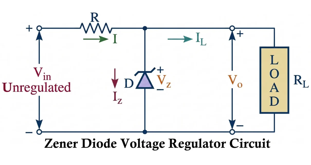
A Zener diode voltage regulator circuit is one of the simplest and most widely used voltage regulator in electronics. It employs a reverse-biased Zener diode operating in its breakdown region to maintain a nearly constant output voltage, even when the input supply voltage or load current changes within specified limits.
Electronic circuits such as microcontrollers, sensors, communication modules, operational amplifiers, and digital ICs require a stable DC supply voltage for reliable operation. Variations in the input supply or changes in load current can cause fluctuations in the output voltage, leading to improper operation or even permanent damage to sensitive electronic components.
A Zener diode regulator solves this problem by automatically adjusting the current flowing through the Zener diode while keeping the voltage across the load almost constant. This makes it an inexpensive and reliable solution for low-power voltage regulation and voltage reference applications.
The circuit is classified as a shunt voltage regulator because the Zener diode is connected in parallel (shunt) with the load. A series resistor is connected between the input supply and the Zener diode to limit the current and protect the diode from excessive power dissipation.
Compared to transistor-based or integrated voltage regulators, a Zener regulator is simple to design, requires very few components, and is suitable for low-current applications where high efficiency is not a primary requirement.
Characteristics of Zener Diode Voltage Regulator:
- Provides a nearly constant output voltage over a specified input voltage range.
- Uses a reverse-biased Zener diode operating in its breakdown region.
- Requires only one series current-limiting resistor in addition to the Zener diode.
- Offers excellent simplicity, low cost, and high reliability.
- Best suited for low-power voltage regulation and voltage reference circuits.
- Protects sensitive electronic circuits from voltage fluctuations.
Note: The Zener diode regulates the output voltage only when its operating current remains between the minimum Zener current (IZK) and the maximum allowable Zener current (IZM).
Related Articles:
- LM317 adjustable voltage regulator circuit
- Difference Between Surge Protection and Over Voltage Protection
- Zener Diode: Symbol, Construction, Working, Types and Applications
- Types of Diodes: Symbol, Working, Characteristics and Applications
- Difference Between Photodiode, Phototransistor and Photoresistor
- Constant Current Diode Symbol, Construction, Working & Applications
- Diode Clipper Circuit Diagram, Types, Working and Applications
- Diode Clamper Circuit Diagram, Types, Working and Applications
- TVS Diode: Symbol, Construction, Working, Types and Applications
- LED – Symbol, Construction, Working, Types and Applications
- Laser Diode – Symbol, Construction, Working, Types & Applications
Circuit Diagram of Zener Voltage Regulator
The basic Zener diode voltage regulator consists of a DC input supply, a current-limiting resistor, a reverse-biased Zener diode, and a load resistance connected across the Zener diode.

In the circuit:
- VIN = Unregulated DC input voltage.
- R = Series current-limiting resistor.
- ZD = Reverse-biased Zener diode.
- RL = Load resistance.
- VO = Regulated output voltage.
The series resistor performs two important functions:
- Limits the current through the Zener diode during reverse breakdown.
- Drops the excess input voltage that is greater than the Zener voltage.
Since the load is connected directly across the Zener diode, both experience the same voltage.
Therefore,
VO = VZ
- VO = Output voltage
- VZ = Zener breakdown voltage
The total current supplied by the source divides into two parts:
I = IZ + IL
- I = Current through the series resistor
- IZ = Current through the Zener diode
- IL = Load current
The current flowing through the series resistor is given by:
I = (VIN − VZ) / RS
Similarly, the load current is
IL = VO / RL = VZ / RL
These relationships form the basis for designing and analyzing every Zener diode voltage regulator circuit.
Principle of Operation
The operation of a Zener diode voltage regulator is based on the unique reverse breakdown characteristic of the Zener diode.
When a conventional PN junction diode is reverse biased, only a very small leakage current flows through it. However, a Zener diode is specially manufactured with a heavily doped PN junction so that it can safely operate in the reverse breakdown region without being damaged.

As the reverse voltage across the diode increases and reaches the Zener breakdown voltage (VZ), the diode starts conducting a large reverse current. Unlike an ordinary diode, the voltage across the Zener diode remains almost constant even though the current changes over a wide range.
This property allows the Zener diode to behave as a constant-voltage device.
When connected across the load, the Zener diode automatically absorbs any excess current caused by variations in the input voltage or load current. As a result, the voltage across the load remains nearly constant.
The regulation mechanism can be summarized as follows:
- If the input voltage increases, the current through the series resistor increases.
- The additional current flows through the Zener diode.
- The output voltage remains approximately equal to the Zener voltage.
- If the input voltage decreases, the Zener current decreases automatically.
- As long as the Zener current remains above the knee current (IZK), voltage regulation is maintained.
Thus, the Zener diode continuously adjusts its reverse current to compensate for variations in supply voltage while maintaining a stable output voltage across the load.
Working of Zener Diode as a Voltage Regulator
The working of a Zener diode voltage regulator can be understood by considering the current flow through the circuit after the input voltage is applied.
Initially, when the input voltage is lower than the Zener breakdown voltage, the diode remains in the reverse leakage region and conducts only a very small current. Under this condition, the output voltage is not regulated.
As the input voltage increases and reaches the breakdown voltage of the Zener diode, the diode enters its reverse breakdown region and begins conducting a significant reverse current. The voltage across the Zener diode quickly stabilizes at approximately its rated breakdown voltage.
Since the load resistance is connected in parallel with the Zener diode, the load voltage also becomes constant.
VO ≈ VZ
The series resistor limits the total current supplied by the source.
This current is shared between the load and the Zener diode.
I = IL + IZ
During normal operation:
- The load receives only the current required by the load resistance.
- The remaining current flows through the Zener diode.
- The Zener diode automatically adjusts its current to keep the output voltage nearly constant.
For proper voltage regulation, the operating current through the Zener diode must always satisfy:
IZK ≤ IZ ≤ IZM
- IZK = Minimum Zener (knee) current required to maintain regulation.
- IZM = Maximum safe Zener current determined by the power rating of the diode.
If the Zener current falls below IZK, the diode leaves the breakdown region and the output voltage begins to decrease.
If the Zener current exceeds IZM, excessive power is dissipated in the diode, which may cause overheating and permanent damage.
Therefore, selecting the proper value of the series resistor is one of the most important design considerations in a Zener voltage regulator. The resistor must ensure that the Zener current always remains within its specified operating range under all expected input voltage and load conditions.
Important: A Zener regulator provides good voltage regulation only when the input voltage is higher than the Zener voltage and the Zener diode continuously operates within its specified current and power ratings.
Regulation with Varying Input Voltage (Line Regulation)
In practical power supplies, the input voltage is rarely constant. It may increase or decrease due to fluctuations in the AC mains supply, transformer regulation, battery discharge, or variations in the power source. Despite these changes, many electronic circuits require a stable output voltage for reliable operation.
The ability of a Zener diode regulator to maintain a constant output voltage when the input voltage changes while the load remains constant is known as Line Regulation.

In this condition:
- The load resistance RL remains constant.
- The Zener voltage VZ remains approximately constant.
- The output voltage remains nearly constant.
- The Zener diode automatically adjusts its current to compensate for changes in the input voltage.
Since the Zener diode is operating in the reverse breakdown region,
VO = VZ = Constant
The load current is therefore,
IL = VO / RL = VZ / RL
Because both VZ and RL remain constant,
IL = Constant
The total current supplied by the source is
I = (VIN − VZ) / RS
and
I = IZ + IL
Since the load current remains constant, any change in the source current is absorbed entirely by the Zener diode.

Case 1: Input Voltage Increases
Suppose the input voltage increases while the load remains unchanged.
- The voltage drop across the series resistor increases.
- The current through the series resistor increases.
- Since the load current remains constant, the extra current flows through the Zener diode.
- The Zener current IZ increases.
- The output voltage remains approximately equal to the Zener voltage.
Therefore,
VIN ↑ → I ↑ → IZ ↑ → VO ≈ Constant
Case 2: Input Voltage Decreases
When the input voltage decreases,
- The voltage across the series resistor decreases.
- The total current supplied by the source decreases.
- The load current remains unchanged.
- The Zener diode automatically reduces its current.
- The output voltage remains constant as long as the Zener current stays above the knee current.
Therefore,
VIN ↓ → I ↓ → IZ ↓ → VO ≈ Constant
Condition for Proper Line Regulation
For satisfactory voltage regulation, the Zener current must always remain within its permissible operating range.
IZK ≤ IZ ≤ IZM
- IZK = Minimum Zener (knee) current required for regulation.
- IZM = Maximum safe Zener current.
If the Zener current falls below IZK, the diode leaves the breakdown region and voltage regulation is lost.
If the Zener current exceeds IZM, the power dissipation may exceed the rated value, causing overheating and possible failure of the diode.
The maximum power dissipated by the Zener diode is given by
PZ = VZ × IZ
For safe operation,
PZ ≤ PD(max)
Key Point: During line regulation, the load current remains constant, while the Zener current automatically increases or decreases to compensate for variations in the input voltage and maintain a constant output voltage.
Regulation with Varying Load Resistance (Load Regulation)
In many electronic systems, the load connected to the power supply is not constant. As the load changes, the load current also changes. A good voltage regulator must maintain a constant output voltage even when the load current varies.
The ability of a Zener diode regulator to maintain a constant output voltage when the load resistance or load current changes while the input voltage remains constant is known as Load Regulation.

Under this operating condition:
- The input voltage VIN remains constant.
- The series resistor RS remains fixed.
- The total current supplied by the source remains nearly constant.
- The Zener diode adjusts its current automatically to accommodate changes in the load current.
The current through the series resistor is
I = (VIN − VZ) / RS
Since both VIN and RS are constant,
I = Constant
The total current is divided between the load and the Zener diode.
I = IL + IZ
Thus, whenever the load current changes, the Zener current changes in the opposite direction.

Case 1: Load Resistance Decreases
If the load resistance decreases,
- The load current increases.
- The total current supplied by the source remains constant.
- The Zener current decreases by the same amount.
- The output voltage remains approximately constant.
Therefore,
RL ↓ → IL ↑ → IZ ↓ → VO ≈ Constant
Case 2: Load Resistance Increases
If the load resistance increases,
- The load current decreases.
- The excess current is diverted through the Zener diode.
- The Zener current increases.
- The regulated output voltage remains constant.
Therefore,
RL ↑ → IL ↓ → IZ ↑ → VO ≈ Constant
Condition for Proper Load Regulation
For proper regulation, the Zener current must always remain within its specified operating limits.
IZK ≤ IZ ≤ IZM
If the load current becomes excessively large, the Zener current may fall below IZK, causing the diode to leave the breakdown region and resulting in a drop in the regulated output voltage.
Similarly, if the load current becomes very small or the load is disconnected, nearly all of the source current flows through the Zener diode. If this current exceeds IZM, the diode may be damaged due to excessive power dissipation.
Therefore, the series resistor must be selected carefully so that the Zener diode always operates safely under both no-load and full-load conditions.
Key Point: During load regulation, the input current remains nearly constant, while the Zener diode continuously adjusts its current in the opposite direction of the load current to maintain a stable output voltage.
Zener Diode Specifications and Ratings
The performance of a Zener diode voltage regulator depends not only on the circuit design but also on the electrical characteristics of the selected Zener diode. Manufacturers specify these characteristics in the device datasheet, allowing engineers to choose a diode that provides stable voltage regulation under different input voltages, load conditions, and operating temperatures.
Before designing a Zener diode voltage regulator, it is important to understand the key specifications and ratings of the Zener diode. These parameters determine the allowable operating current, power dissipation, voltage accuracy, temperature stability, and overall reliability of the regulator circuit.
Nominal Zener Voltage (VZ or VZT)
The Nominal Zener Voltage is the reverse breakdown voltage of the Zener diode measured at a specified test current.
It is the voltage that appears across the diode when it operates in the reverse breakdown region.
- Represented by VZ or VZT.
- Specified at a particular Zener test current IZT.
- Available in standard values ranging from approximately 2.4 V to over 200 V.
- Acts as the regulated output voltage in voltage regulator circuits.
Examples: 3.3 V Zener Diode, 5.1 V Zener Diode, 6.8 V Zener Diode, 12 V Zener Diode, 24 V Zener Diode
Zener Test Current (IZT)
The Zener Test Current is the reverse current at which the nominal Zener voltage is measured and specified.
Manufacturers use this current as a reference point for specifying various diode parameters.
- Represented by IZT.
- Specified in the datasheet.
- Used for measuring nominal Zener voltage.
- Used for determining dynamic impedance.
At this current:
VZ = Rated Zener Voltage
Minimum Zener Current (IZ(min) or IZK)
The minimum current required to maintain the diode in the breakdown region is known as the Minimum Zener Current.
It corresponds to the knee point of the V-I characteristic curve.
- Represented by IZK or IZ(min).
- Also called Knee Current.
- Indicates the beginning of the Zener breakdown region.
- Below this current, proper voltage regulation may not be achieved.
For proper operation:
IZ ≥ IZK
Maximum Zener Current (IZM or IZ(max))
The maximum current that a Zener diode can safely conduct without exceeding its power rating is called the Maximum Zener Current.
- Represented by IZM or IZ(max).
- Determined by the power dissipation capability of the diode.
- Exceeding this current can cause overheating and permanent damage.
The operating current must satisfy:
IZK ≤ IZ ≤ IZM
Dynamic Zener Resistance (ZZ or ZZT)
In practice, the reverse breakdown characteristic of a Zener diode is not perfectly vertical. A small change in current causes a slight change in voltage.
This effect is represented by the Dynamic Zener Resistance.
It is defined as:
ZZ = ΔVZ / ΔIZ
- ZZ = Dynamic resistance (Ω)
- ΔVZ = Change in Zener voltage
- ΔIZ = Change in Zener current
- Also known as Zener Impedance.
- Usually specified at the test current IZT.
- A lower value indicates better voltage regulation.
Maximum Power Dissipation (PD(max))
The maximum power that a Zener diode can dissipate safely without damage is called the Maximum Power Dissipation.
It is given by:
PD(max) = VZ × IZM
- PD(max) = Maximum power dissipation (W)
- VZ = Zener voltage (V)
- IZM = Maximum Zener current (A)
Common power ratings include: 250 mW, 500 mW, 1 W, 3 W, 5 W, 10 W, 50 W and higher
For safe operation:
PZ ≤ PD(max)
Reverse Leakage Current (IR)
The small current flowing through the Zener diode before breakdown occurs is called the Reverse Leakage Current.
- Represented by IR.
- Measured at a specified reverse voltage below breakdown.
- Typically in the microampere (μA) range.
- Increases with temperature.
Ideally IR ≈ 0, but practical diodes always exhibit a small leakage current.
Zener Voltage Tolerance
The actual breakdown voltage of a manufactured diode may vary slightly from its nominal value.
This variation is specified as Zener Voltage Tolerance.
- Indicates the permissible deviation from the nominal voltage.
- Expressed as a percentage.
- Lower tolerance values provide better accuracy.
Typical Tolerance Values: ±10%, ±5%, ±2%, ±1%
Example: A 5.1 V Zener diode with ±5% tolerance may have an actual breakdown voltage between 4.845 V to 5.355 V.
Temperature Coefficient (TC)
The Temperature Coefficient indicates how the Zener voltage changes with temperature. It is usually expressed in mV/°C or %/°C.
- Low-voltage Zener diodes generally have a negative temperature coefficient.
- High-voltage Zener diodes generally have a positive temperature coefficient.
- Approximately 5.6 V Zener diodes exhibit near-zero temperature coefficient and excellent stability.
Junction Capacitance (CJ)
Like all PN junction devices, a Zener diode possesses junction capacitance.
- Represented by CJ.
- Measured under reverse-bias conditions.
- Depends on the depletion region width.
- Important in high-frequency applications.
The junction capacitance decreases as the reverse voltage increases.
Maximum Reverse Surge Current
Some Zener diodes are capable of handling short-duration surge currents.
This rating specifies the maximum surge current the device can withstand safely without damage.
It is important in transient protection circuits, power supply protection and industrial control systems.
Zener Diode Specifications
| Parameter | Symbol | Description |
|---|---|---|
| Nominal Zener Voltage | VZ | Rated breakdown voltage |
| Zener Test Current | IZT | Current at which VZ is specified |
| Minimum Zener Current | IZK | Minimum current required for regulation |
| Maximum Zener Current | IZM | Maximum safe operating current |
| Dynamic Resistance | ZZ | Small-signal resistance in breakdown region |
| Maximum Power Dissipation | PD(max) | Maximum allowable power |
| Reverse Leakage Current | IR | Leakage current before breakdown |
| Temperature Coefficient | TC | Change in VZ with temperature |
| Junction Capacitance | CJ | PN junction capacitance |
| Voltage Tolerance | ±% | Permissible variation in VZ |
- The most important datasheet parameters are VZ, IZT, IZK, IZM, and PD(max).
- The Zener diode must always operate between IZK and IZM.
- Dynamic resistance determines the quality of voltage regulation.
- Power dissipation rating must never be exceeded.
- Temperature coefficient and tolerance are critical for precision voltage reference applications.
Designing Zener Voltage Regulator
Designing a Zener diode voltage regulator involves selecting an appropriate Zener diode and calculating the correct value of the series resistor so that the diode always operates within its safe operating region. The regulator should maintain a constant output voltage under all expected variations in input voltage and load current.
Design Procedure
- Select the desired output voltage.
- Choose a Zener diode having the same breakdown voltage.
- Calculate the maximum load current.
- Select the minimum operating Zener current.
- Calculate the series resistor.
- Verify Zener current limits.
- Check Zener power dissipation.
- Select the nearest standard resistor and suitable Zener power rating.
The design must ensure that:
- The output voltage remains equal to the Zener voltage.
- The Zener diode always operates in the reverse breakdown region.
- The Zener current never falls below the minimum knee current (IZK).
- The Zener current never exceeds the maximum allowable current (IZM).
- The Zener diode power dissipation remains below its rated value.
Step 1: Select the Required Output Voltage
The first step is to determine the regulated output voltage required by the load.
Choose a Zener diode whose nominal breakdown voltage is equal to the desired output voltage.
VO = VZ
Example: For a required output voltage of 5V select 5V to 5.1V Zener Diode.
Step 2: Determine the Load Current
If the load resistance is known, calculate the load current using Ohm’s law.
IL = VO / RL
- IL = Load current
- VO = Output voltage
- RL = Load resistance
If the load current is already specified, this step can be skipped.
Step 3: Calculate the Series Resistor
The series resistor limits the current flowing through both the load and the Zener diode.
The resistor value is calculated using
RS = (VIN − VZ) / (IL + IZ)
- RS = Series resistor (Ω)
- VIN = Input voltage (V)
- VZ = Zener voltage (V)
- IL = Load current (A)
- IZ = Desired operating Zener current (A)
Usually, the selected Zener operating current is greater than the knee current to ensure stable regulation.
Step 4: Verify the Zener Current Limits
After selecting the resistor, verify that the Zener current remains within its safe operating limits under all operating conditions.
IZK ≤ IZ ≤ IZM
- IZK = Minimum regulating current.
- IZM = Maximum allowable current.
If this condition is not satisfied, choose another resistor value or a different Zener diode.
Step 5: Verify the Zener Power Rating
The maximum power dissipated by the Zener diode is
PZ = VZ × IZ(max)
The selected diode must satisfy
PZ ≤ PD(max)
PD(max) is the rated power dissipation specified in the datasheet. If the calculated power exceeds the rated value, select a higher power Zener diode.
Practical Design Example 1
Design Specification
- Input Voltage = 12 V
- Required Output Voltage = 5.1 V
- Load Current = 20 mA
- Desired Zener Current = 10 mA
Step 1: Select the Zener Diode
VZ = 5.1 V
Step 2: Calculate Total Current
I = IL + IZ
= 20 mA + 10 mA = 30 mA
Step 3: Calculate Series Resistance
RS = (12 − 5.1)/0.03 = 230 Ω
Select the nearest preferred resistor value
RS = 220 Ω or 240 Ω
Step 4: Verify Zener Power
PZ = 5.1 × 0.01 = 0.051 W = 51 mW
Therefore, even a 250 mW Zener diode can safely handle the required power.
Practical Design Example 2
Design Specification
- Zener Voltage = 12 V
- Input Voltage = 18 V
- Load Resistance = 240 Ω
- Minimum Zener Current = 8 mA
Step 1: Calculate Load Current
IL = 12 / 240 = 50 mA
Step 2: Minimum Required Source Current
I = IL + IZK
= 50 + 8 = 58 mA
Step 3: Calculate Series Resistance
RS = (18 − 12)/0.058 ≈ 103 Ω
Select the nearest standard resistor value
RS = 100 Ω
The regulator will maintain approximately 12 V across the load as long as the Zener diode remains within its specified operating current range.
Design Considerations
Although a Zener diode voltage regulator is simple to implement, careful component selection is essential to obtain stable voltage regulation, long-term reliability, and safe operation. The following design considerations should always be taken into account.
- Select the Correct Zener Voltage
Choose a Zener diode whose nominal breakdown voltage is equal to the required regulated output voltage.VZ ≈ VO
Using an incorrect Zener voltage will result in an incorrect output voltage.
- Choose the Proper Series Resistor
The series resistor is one of the most critical components in the regulator circuit. It should limit the current through the Zener diode, provide sufficient current for the load, and maintain the Zener current within its specified operating range. An incorrect resistor value may cause poor regulation or damage the Zener diode. - Keep the Zener Current Within Safe Limits
Always ensureIZK ≤ IZ ≤ IZM
Operating below the knee current causes regulation failure, while operating above the maximum current may permanently damage the diode.
- Verify Power Dissipation
The maximum power dissipated by the Zener diode should always remain below its rated value.PZ = VZ × IZ
A safety margin of 20–50% is generally recommended when selecting the diode power rating.
- Consider Maximum Input Voltage
Always perform calculations using the highest expected input voltage because this condition produces the maximum Zener current and maximum power dissipation. - Consider Minimum Input Voltage
Verify that the Zener current remains above the knee current when the input voltage falls to its minimum specified value. - Account for Load Variations
The regulator should be designed so that proper regulation is maintained under both no-load and full-load conditions. - Temperature Effects
The Zener voltage changes slightly with temperature. For precision voltage reference circuits, choose Zener diodes with low temperature coefficient, tight voltage tolerance, and high stability. Approximately 5.6 V Zener diodes generally exhibit the lowest temperature coefficient. - Resistor Power Rating
The series resistor also dissipates power. Calculate its power rating usingPR = I²R
PR = (VIN − VZ) × I
Always select a resistor with a power rating greater than the calculated value.
- Efficiency
Since the Zener diode continuously draws current, even under light-load conditions, the overall efficiency of a Zener regulator is relatively low. For high-current or high-efficiency applications, transistor regulators or integrated voltage regulators are generally preferred. - Best Practices
- Select the Zener diode based on both voltage and power ratings.
- Verify circuit operation under minimum and maximum input voltage conditions.
- Consider worst-case load current during design.
- Provide adequate safety margin for both resistor and Zener power ratings.
- Use proper heat dissipation for high-power Zener diodes.
- Always consult the manufacturer’s datasheet before finalizing the design.
Advantages of Zener Diode Voltage Regulator
The Zener diode voltage regulator is widely used in low-power electronic circuits because of its simple design, low cost, and reliable voltage regulation. Although it cannot provide the high efficiency of modern integrated voltage regulators, it remains an excellent choice for many basic voltage regulation and reference applications.
The major advantages of a Zener diode voltage regulator are listed below.
- Simple Circuit Design: The regulator requires only a Zener diode and a series resistor, making the circuit extremely simple to design, assemble, and troubleshoot.
- Low Cost: Since it uses very few inexpensive components, the overall cost of the regulator is much lower than transistor-based or IC voltage regulators.
- Stable Output Voltage: The Zener diode maintains a nearly constant output voltage over a wide range of input voltages and load conditions, provided it operates within its specified current limits.
- Excellent Voltage Reference: Due to its well-defined breakdown voltage, the Zener diode serves as an accurate voltage reference in analog and digital electronic circuits.
- Fast Response: The Zener diode responds almost instantly to changes in input voltage or load current, helping maintain a stable output voltage.
- Good Reliability: With proper current limiting and power dissipation, Zener diode regulators provide long service life and dependable operation.
- Compact Size: The circuit occupies very little PCB space, making it suitable for compact electronic devices.
- Easy Component Selection: Zener diodes are available in a wide range of standard voltage ratings and power ratings, simplifying circuit design.
- Suitable for Low-Power Applications: It is an ideal regulator for low-current circuits such as sensors, signal conditioning circuits, reference voltage sources, and small electronic modules.
- Provides Overvoltage Protection: Besides voltage regulation, the Zener diode can also protect sensitive electronic components by limiting excessive voltage.
Disadvantages of Zener Diode Voltage Regulator
Despite its simplicity and low cost, a Zener diode voltage regulator has several limitations that make it unsuitable for high-power or high-efficiency applications.
The main disadvantages are as follows.
- Low Efficiency: The Zener diode continuously draws current even when the load current is small, resulting in unnecessary power loss.
- Limited Output Current: Zener diode regulators are suitable only for low-current applications. High load currents require larger power-rated Zener diodes and result in significant power dissipation.
- Poor Efficiency at Light Load: When the load current decreases, a larger portion of the current flows through the Zener diode, increasing power dissipation without performing useful work.
- Heat Generation: Excess electrical energy is converted into heat in both the series resistor and the Zener diode, especially when the input voltage is much higher than the output voltage.
- Limited Regulation Accuracy: The output voltage changes slightly due to the dynamic resistance of the Zener diode and variations in operating current.
- Temperature Dependence: The Zener voltage varies with temperature. In precision applications, this temperature coefficient may affect voltage accuracy.
- Not Suitable for Large Input Voltage Variations: Very large changes in input voltage may force the Zener current outside its safe operating range, causing loss of regulation or device failure.
- Requires Careful Resistor Selection: Incorrect selection of the series resistor can lead to insufficient regulation or excessive power dissipation.
- Limited Output Voltage Precision: Manufacturing tolerances result in slight variations in the actual breakdown voltage of practical Zener diodes.
- Unsuitable for High-Power Supplies: For medium- and high-power power supplies, transistor regulators, switching regulators, or integrated voltage regulators are much more efficient.
Applications of Zener Diode Voltage Regulator
Due to its simplicity, low cost, and ability to provide a stable reference voltage, the Zener diode voltage regulator is widely used in analog, digital, industrial, automotive, and communication electronics. Although modern integrated voltage regulators are preferred for high-current applications, Zener regulators continue to play an important role in numerous low-power circuits.
Some of the most common applications are listed below.
- Low-Power DC Voltage Regulation: Used to provide a constant DC output voltage for small electronic circuits operating at low current.
- Voltage Reference Circuits: Used as a precise reference voltage in operational amplifiers, comparators, analog-to-digital converters (ADC), digital-to-analog converters (DAC), and measurement instruments.
- Power Supply Circuits: Used in linear power supplies to stabilize the output voltage and reduce the effects of supply voltage fluctuations.
- Overvoltage Protection: Protects electronic components from excessive voltage by limiting the maximum voltage across the load.
- Voltage Clamping and Clipping Circuits: Used in clipper and clamper circuit to limit signal amplitudes and protect sensitive input stages in communication and signal-processing circuits.
- Microcontroller and Embedded Systems: Provides stable reference voltages and protects I/O pins from overvoltage conditions.
- Instrumentation Circuits: Used in voltmeters, digital multimeters, oscilloscopes, and other precision measuring instruments.
- Sensor Interface Circuits: Supplies stable reference voltages required for accurate sensor operation and signal conditioning.
- Transistor Bias Stabilization: Maintains a constant bias voltage in transistor amplifier circuits, improving operating stability.
- Battery-Powered Devices: Used in portable electronic equipment where simple and inexpensive voltage regulation is required.
- Communication Equipment: Employed in RF circuits, communication modules, and telecom equipment for voltage stabilization.
- Industrial Control Systems: Used in control circuits, PLC input modules, relay drivers, and monitoring equipment.
- Automotive Electronics: Provides voltage stabilization and transient protection in automotive electronic modules.
- Consumer Electronics: Found in televisions, audio amplifiers, chargers, adapters, set-top boxes, and numerous household electronic products.
Note: While Zener diode voltage regulators are ideal for low-power applications, integrated linear regulators (such as the 78xx series) and switching regulators are generally preferred for applications requiring high output current, better efficiency, or tighter voltage regulation.
Conclusion
A Zener diode voltage regulator is one of the simplest and most effective circuits for obtaining a stable DC output voltage from an unregulated power source. By operating in the reverse breakdown region, the Zener diode maintains an almost constant voltage across the load despite moderate variations in the input voltage or load current.
The operation of the regulator relies on a properly selected series current-limiting resistor, which ensures that the Zener diode always operates within its specified current range. For reliable voltage regulation, the Zener current must remain between the minimum knee current (IZK) and the maximum allowable current (IZM), while the power dissipation must never exceed the diode’s rated power.
Although Zener diode regulators are not suitable for high-current or high-efficiency applications due to continuous power dissipation, they remain an excellent choice for low-power circuits because of their simplicity, low cost, compact size, and dependable performance.
Understanding concepts such as line regulation, load regulation, Zener diode specifications, and practical design calculations enables engineers, students, and electronics enthusiasts to design reliable voltage regulator circuits for a wide range of analog and digital applications.
Whether used as a voltage regulator, voltage reference, overvoltage protector, or signal limiter, the Zener diode continues to be one of the most important semiconductor devices in modern electronics.
Frequently Asked Questions (FAQ)
1. What is a Zener diode voltage regulator?
A Zener diode voltage regulator is a simple shunt regulator circuit that uses a reverse-biased Zener diode to maintain a nearly constant output voltage even when the input voltage or load current changes within specified limits.
2. Why is a Zener diode connected in reverse bias?
A Zener diode regulates voltage only when it operates in its reverse breakdown region. In reverse bias, once the applied voltage reaches the Zener breakdown voltage, the diode conducts while maintaining an almost constant voltage across its terminals.
3. Why is a series resistor required in a Zener regulator?
The series resistor limits the current flowing through the Zener diode and the load. Without this resistor, excessive current could flow through the Zener diode during breakdown, causing overheating and permanent damage.
4. What is the output voltage of a Zener diode regulator?
The regulated output voltage is approximately equal to the Zener breakdown voltage. VO ≈ VZ
5. What is line regulation?
Line regulation is the ability of the regulator to maintain a constant output voltage when the input voltage changes while the load remains constant.
6. What is load regulation?
Load regulation is the ability of the regulator to maintain a constant output voltage when the load current or load resistance changes while the input voltage remains constant.
7. What happens if the Zener current falls below the knee current?
If the Zener current becomes less than the knee current (IZK), the diode leaves the breakdown region and the output voltage is no longer properly regulated.
8. What if Zener current exceeds the maximum allowable value?
When the Zener current exceeds IZM, the power dissipation increases beyond the diode’s rating, which may cause excessive heating and permanent damage.
9. How is the series resistor calculated in a Zener regulator?
The required series resistor is calculated using
RS = (VIN − VZ) / (IL + IZ)
- VIN = Input voltage
- VZ = Zener voltage
- IL = Load current
- IZ = Desired Zener current
10. How is the maximum power dissipation of a Zener diode calculated?
The maximum power dissipated by the Zener diode is
PZ = VZ × IZ
The calculated value must always be less than or equal to the rated power specified in the datasheet.
11. Why is a 5.6 V Zener diode commonly preferred?
A Zener diode with a breakdown voltage of approximately 5.6 V has a temperature coefficient close to zero. This provides excellent voltage stability over a wide temperature range, making it ideal for precision voltage reference applications.
12. Can a Zener diode regulator supply high current?
No. A basic Zener diode regulator is intended for low-power and low-current applications. High-current loads require transistor-based regulators, integrated linear regulators, or switching regulators.
13. What are the main applications of a Zener diode voltage regulator?
Common applications include:
- Low-power DC voltage regulation
- Voltage reference circuits
- Overvoltage protection
- Clipping and clamping circuits
- Instrumentation systems
- Microcontroller and embedded systems
- Power supply circuits
14. What are the advantages of a Zener diode voltage regulator?
Some important advantages include:
- Simple circuit design
- Low cost
- Compact size
- Reliable operation
- Stable output voltage
- Excellent voltage reference characteristics
15. What are the limitations of a Zener diode voltage regulator?
Its major limitations are:
- Low efficiency
- Continuous power dissipation
- Limited output current capability
- Heat generation
- Not suitable for high-power applications
16. How do I choose the correct Zener diode?
When selecting a Zener diode, consider:
- Required output voltage (VZ)
- Power rating (PD(max))
- Maximum and minimum operating current
- Voltage tolerance
- Temperature coefficient
- Package type and thermal characteristics
Choosing a diode that satisfies all these specifications ensures safe operation, reliable voltage regulation, and long service life.
Zener Diode: Symbol, Construction, Working, Types and Applications
Difference Between Surge Protection and Over Voltage Protection
Types of Diodes: Symbol, Working, Characteristics and Applications
Light Emitting Diode LED – Symbol, Construction, Working, Types and Applications
Diode Clipper Circuit Diagram, Types, Working and Applications
Diode Clamper Circuit Diagram, Types, Working and Applications

