A PN junction is one of the most important structures in semiconductor electronics. It forms the basic building block of many electronic devices such as diodes, transistors, LEDs, solar cells, rectifiers, and integrated circuits. When a P-type semiconductor and an N-type semiconductor are joined together without applying any external voltage, the junction is called an unbiased PN junction.
In this condition, important phenomena such as diffusion, recombination, depletion region formation, and barrier potential are developed naturally inside the semiconductor material. These effects control the electrical behavior of the PN junction diode.
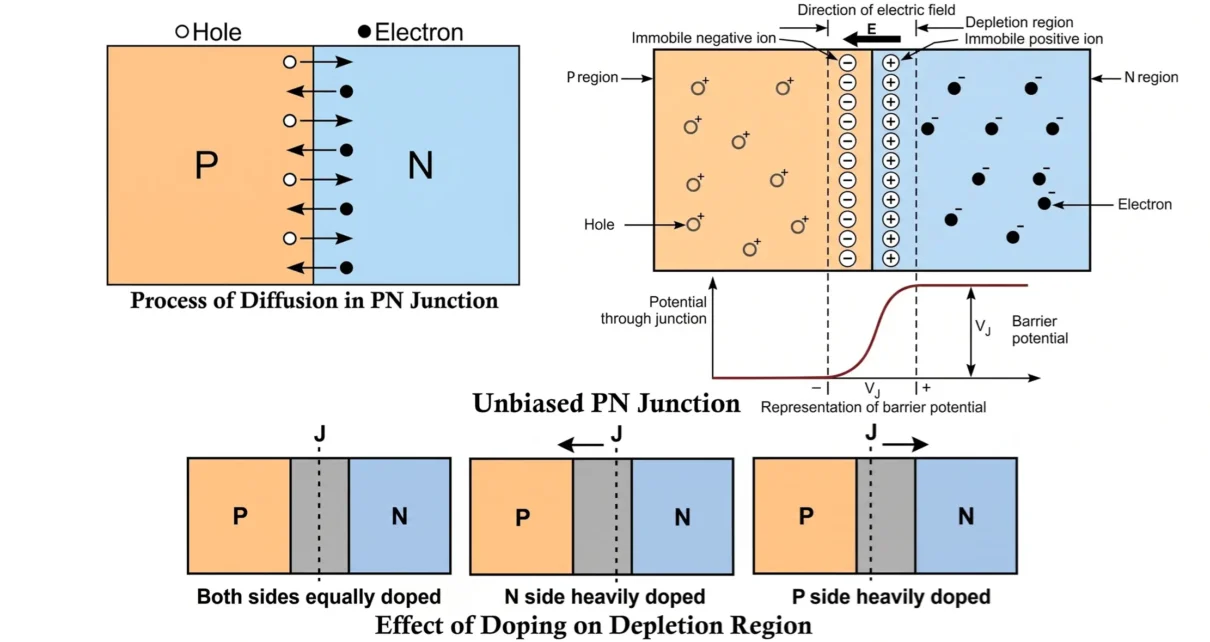
What is an Unbiased PN Junction?
An unbiased PN junction is formed when a P-type semiconductor and an N-type semiconductor are connected together without any external battery or voltage source.
- The P-region contains a large number of holes as majority charge carriers.
- The N-region contains a large number of free electrons as majority charge carriers.
Due to the difference in charge carrier concentration on both sides, the charge carriers start moving across the junction automatically.
Related Articles:
- Intrinsic Semiconductors Explained
- Extrinsic Semiconductors Explained
- Drift Current and Diffusion Current in Semiconductors
- Difference Between Intrinsic and Extrinsic Semiconductor
- LED – Symbol, Construction, Working, Types and Applications
- Energy Band Theory of Solids: Conductors, Semiconductors, and Insulators
Formation of PN Junction
A PN junction is created by doping a single crystal semiconductor material such as silicon or germanium in such a way that:
- One side becomes P-type by adding trivalent impurities.
- The other side becomes N-type by adding pentavalent impurities.
At the junction boundary holes are highly concentrated on the P-side and electrons are highly concentrated on the N-side. Because of this concentration difference, diffusion begins immediately after the junction is formed.
Diffusion Process in PN Junction
In semiconductor materials, charge carriers always try to move from a region of higher concentration to a region of lower concentration. This movement is known as diffusion.

- Electron Diffusion
- The N-side contains a large number of free electrons.
- The P-side contains very few electrons.
- Therefore, electrons diffuse from the N-region toward the P-region.
- Hole Diffusion
- The P-side contains a large number of holes.
- The N-side contains very few holes.
- Hence, holes diffuse from the P-region toward the N-region.
This initial movement of charge carriers is called the diffusion current.
Recombination Process
When electrons cross the junction and enter the P-region they recombine with holes present there. Similarly, when holes enter the N-region they recombine with free electrons. As recombination takes place near the junction free mobile carriers disappear in that region and charged ions are left behind.
Formation of Depletion Region
After recombination donor atoms near the junction on the N-side lose electrons and become positive immobile ions and acceptor atoms near the junction on the P-side gain electrons and become negative immobile ions.
Since these ions cannot move, they remain fixed near the junction. As more electrons and holes diffuse and recombine, a region forms around the junction where no free charge carriers exist.

This region is called Depletion Region, Depletion Layer or Space Charge Region.
Why is it Called Depletion Region? The region is called depletion region because it is depleted of free electrons and free holes. Only immobile ions remain inside this region.
Properties of Depletion Region
- No Free Charge Carriers: The depletion region does not contain mobile electrons and mobile holes.
- Presence of Immobile Ions: It contains negative immobile ions on the P-side and positive immobile ions on the N-side.
- Acts as an Insulating Barrier: The depletion region opposes the further movement of charge carriers across the junction.
- Very Small Width: The depletion layer width is extremely small. Typical depletion width is of the order of a few micrometers. 1 Micron = 1 × 10⁻⁶ m
Electric Field in Depletion Region
The opposite charges on both sides create an electric field across the depletion layer. Positive ions exist on the N-side and negative ions exist on the P-side.
Hence, the electric field direction is from the N-side toward the P-side. This electric field opposes further diffusion of charge carriers.
Effect of Doping on Depletion Region
The width of the depletion region depends on the doping level of both sides. The depletion region penetrates more into the lightly doped side.

- Equal Doping: If both sides are equally doped, depletion width becomes equal on both sides.
- Heavily Doped N-side: If the N-region is heavily doped, depletion region extends more into the P-side.
- Heavily Doped P-side: If the P-region is heavily doped, depletion region extends more into the N-side.
Depletion Width Formula
The depletion width of a PN junction is approximately given by:
W = √[(2ε/q) ((1/NA) + (1/ND)) V0]
- W = Width of depletion region
- ε = Permittivity of semiconductor
- q = Electron charge
- NA = Acceptor concentration
- ND = Donor concentration
- V0 = Barrier potential
Barrier Potential of PN Junction
The electric field developed across the depletion region creates a potential difference known as the barrier potential. It is also called Junction Potential, Built-in Potential or Cut-in Voltage.

Definition: Barrier potential is the potential difference developed across the depletion region of an unbiased PN junction due to immobile ions.
Symbol of Barrier Potential: Barrier potential is represented as: VJ, V0, or Vr
Barrier Potential Formula: The barrier potential of a PN junction is given by:
V0 = (kT/q) ln[(NAND)/(ni2)]
- V0 = Barrier potential
- k = Boltzmann constant
- T = Absolute temperature in Kelvin
- q = Charge of electron
- NA = Acceptor impurity concentration
- ND = Donor impurity concentration
- ni = Intrinsic carrier concentration
Typical Barrier Potential Value for Silicon PN Junction is V0 ≈ 0.7 V and for Germanium PN Junction V0 ≈ 0.3 V, these values are at room temperature.
Factors Affecting Barrier Potential
The barrier potential depends on several factors:
- Type of Semiconductor: Different semiconductor materials produce different barrier voltages. Silicon has higher barrier potential, and Germanium has Lower.
- Doping Concentration: Higher doping concentration increases the barrier potential.
- Temperature: As temperature increases barrier potential decreases.
- Intrinsic Carrier Concentration: Barrier potential depends on the intrinsic carrier density of the semiconductor material.
Thermal Equilibrium in PN Junction
A PN junction reaches thermal equilibrium when diffusion current becomes equal to drift current and net current flows across the junction is zero.
At equilibrium:
Idiffusion = Idrift
Net Current = 0
Drift Current in PN Junction: The electric field in the depletion region causes minority charge carriers to move across the junction. This movement produces drift current. Drift current direction is opposite to diffusion current. In equilibrium condition, both currents balance each other.
Unbiased PN Junction Summary
An unbiased PN junction can be summarized as follows:
- Majority carriers diffuse across the junction.
- Recombination takes place near the junction.
- Immobile ions are formed.
- Depletion region develops.
- Electric field is established.
- Barrier potential is created.
- Diffusion and drift currents balance each other.
- Thermal equilibrium is achieved.
Characteristics of Unbiased PN Junction
- No external voltage is applied.
- Depletion layer exists naturally.
- Barrier potential prevents further diffusion.
- Net current across the junction is zero.
- Electric field exists inside depletion region.
- Width of depletion layer depends on doping concentration.
Advantages of PN Junction
- Simple semiconductor structure
- Fast switching operation
- Low power consumption
- High reliability
- Essential for modern electronics
Disadvantages of PN Junction
- Sensitive to temperature variations
- Barrier potential causes voltage drop
- Depletion region limits carrier flow
- Performance affected by improper doping
Applications of PN Junction
The PN junction principle is used in many electronic devices:
- Rectifier Diodes: Convert AC into DC and are widely used in power supply circuits.
- Zener Diodes: Maintain a constant voltage and are commonly used for voltage regulation.
- LEDs: Emit light when forward biased and are used in displays and lighting systems.
- Photodiodes: Convert light energy into electrical current for sensing applications.
- Solar Cells: Generate electrical energy directly from sunlight through the photovoltaic effect.
- Bipolar Junction Transistors: Used for signal amplification and electronic switching operations.
- Varactor Diodes: Provide voltage-controlled capacitance in tuning and RF circuits.
- Constant Current Diode: Delivers nearly constant current over a specified voltage range.
- Avalanche Diode: Operates in avalanche breakdown and protects circuits from voltage surges.
- Fast Recovery Diode: Features short reverse recovery time for high-frequency switching applications.
- Step Recovery Diode: Produces sharp voltage pulses and is used in frequency multiplier circuits.
- PIN Diode: Commonly used as an RF switch, attenuator, and photodetector.
- TVS Diode: Protects electronic circuits from transient voltage spikes and ESD events.
- Laser Diode: Produces coherent laser light for communication, scanning, and optical storage.
- Schottky Diode: Offers low forward voltage drop and fast switching performance.
- Shockley Diode: A four-layer semiconductor device used in triggering and switching circuits.
- Tunnel Diodes: Utilize quantum tunneling and exhibit negative resistance characteristics.
- Integrated Circuits: Combine multiple electronic components on a single semiconductor chip.
Conclusion
An unbiased PN junction is formed by joining P-type and N-type semiconductor materials without applying any external voltage. Due to the concentration difference of charge carriers, diffusion occurs across the junction leading to recombination and formation of immobile ions. This creates a depletion region and establishes an electric field across the junction.
The electric field develops a barrier potential which opposes further movement of charge carriers. Finally, the junction reaches thermal equilibrium where diffusion current and drift current become equal. Understanding the depletion region and barrier potential is fundamental for studying semiconductor diodes, transistors, and all modern electronic devices.
Frequently Asked Questions (FAQs)
What is an unbiased PN junction?
An unbiased PN junction is a PN junction diode with no external voltage source connected across it.
What is depletion region?
The depletion region is the area around the PN junction that contains no free charge carriers.
Why is barrier potential formed?
Barrier potential is formed due to the electric field created by immobile ions near the junction.
What is the barrier voltage of silicon?
The barrier voltage of silicon is approximately 0.7 V at room temperature.
What is the barrier voltage of germanium?
The barrier voltage of germanium is approximately 0.3 V at room temperature.
Why does depletion region extend more into lightly doped side?
The lightly doped side contains fewer charge carriers, so a larger region must be depleted to balance the charges on both sides.
Energy Band Theory of Solids: Conductors, Semiconductors, and Insulators
Light Emitting Diode LED – Symbol, Construction, Working, Types and Applications
