In this article, we will explore intrinsic semiconductors, including their definition, crystal structure, energy band diagram, characteristics, advantages, disadvantages, and applications. An intrinsic semiconductor is a pure semiconductor material without any significant impurity atoms added to it. In intrinsic semiconductors, the number of free electrons and holes are naturally generated due to thermal energy and remain equal in concentration. Materials like silicon and germanium are the most common intrinsic semiconductors used in electronics and semiconductor physics.
Intrinsic semiconductors form the foundation of all modern electronic devices because understanding their behavior is essential before studying extrinsic semiconductors, PN junctions, diodes, transistors, MOSFETs, and integrated circuits.
- Related Articles:
- Extrinsic Semiconductors Explained
- Difference Between Intrinsic and Extrinsic Semiconductor
- Energy Band Theory of Solids: Conductors, Semiconductors, and Insulators
- Types of Diodes: Symbol, Working, Characteristics and Applications
What is an Intrinsic Semiconductor?
An intrinsic semiconductor is a semiconductor in its chemically purest form, containing an extremely small amount of impurities. The impurity concentration is typically less than one impurity atom in 100 million semiconductor atoms.
- The most common intrinsic semiconductor materials are Silicon (Si) and Germanium (Ge).
- Silicon is widely used because of better thermal stability
- Germanium offers higher conductivity but higher leakage current
- In an intrinsic semiconductor:
- No intentional doping is performed
- Electrical conduction occurs naturally
- Free electrons and holes are generated thermally
- Electron concentration equals hole concentration
Definition of Intrinsic Semiconductor
An intrinsic semiconductor is a pure semiconductor material in which electrical conduction takes place due to thermally generated electron-hole pairs without the addition of external impurity atoms.
Characteristics of Intrinsic Semiconductor
Important characteristics of intrinsic semiconductors are:
- Pure semiconductor material
- No intentional impurity atoms
- Equal number of electrons and holes
- Moderate conductivity
- Conductivity increases with temperature
- Acts as an insulator at absolute zero temperature
- Negative temperature coefficient of resistance
- Current conduction occurs due to both electrons and holes
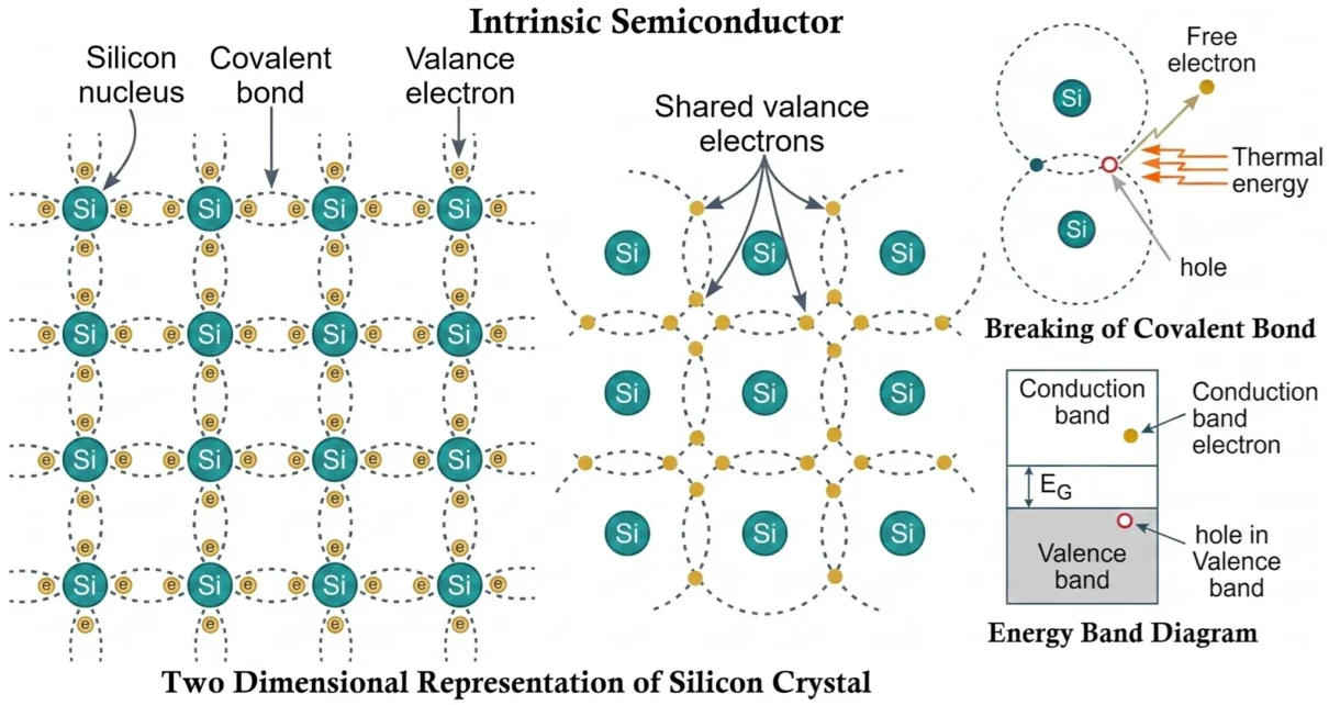
Crystal Structure of Intrinsic Semiconductor
The crystal structure of an intrinsic semiconductor is formed by covalent bonding between neighboring atoms.

- Valence Electrons
- Silicon and germanium atoms contain four electrons in their outermost shell. Therefore, they are called tetravalent atoms.
- Each atom shares its four valence electrons with neighboring atoms to complete the outer shell of eight electrons.
- This sharing of electrons forms covalent bonds.
- Covalent Bond in Semiconductor
- A covalent bond is formed when neighboring atoms share valence electrons with each other.
- In silicon and germanium crystals:
- Each atom forms four covalent bonds
- The crystal becomes stable
- Electrons remain tightly bound at low temperature
- At absolute zero temperature:
- No free electrons exist
- No holes exist
- Semiconductor behaves like an insulator
- Crystal Lattice Structure
- The semiconductor atoms arrange themselves in a highly ordered three-dimensional pattern called a crystal lattice.
- Features of Crystal Structure:
- Uniform arrangement of atoms
- Repetitive lattice structure
- Strong covalent bonding
- Stable atomic arrangement
- Silicon and germanium crystals are generally represented using tetrahedral structures.
Energy Band Theory of Intrinsic Semiconductor
The behavior of intrinsic semiconductors is explained using energy band theory.
- The two important energy bands are valence band and conduction band
- These bands are separated by an energy gap called the forbidden energy gap or band gap.
- Valence Band
- The valence band contains valence electrons that are involved in covalent bonding.
- Electrons are tightly bound
- Responsible for bonding
- No current conduction at absolute zero
- Conduction Band
- The conduction band contains free electrons that can move freely and conduct electricity.
- Electrons possess higher energy
- Responsible for electrical conduction
- Electrons move under applied electric field
- Forbidden Energy Gap
- The energy gap between valence band and conduction band is called the forbidden energy gap.
Eg = Ec - Ev
- Eg = Band gap energy
- Ec = Conduction band energy
- Ev = Valence band energy
Band Gap Energy of Semiconductor Materials
| Semiconductor | Band Gap Energy |
|---|---|
| Germanium | 0.72 eV |
| Silicon | 1.1 eV |
Silicon has a larger band gap than germanium, making it more stable at higher temperatures.
Electron and Hole Generation in Intrinsic Semiconductor
At room temperature, thermal energy breaks some covalent bonds.

- As a result:
- Valence electrons gain energy
- Electrons move to conduction band
- Free electrons are generated
- Holes are created in valence band
This process is called thermal generation.
Electron-Hole Pair
When an electron leaves the valence band and enters the conduction band, a hole is left behind.
- This pair is called an electron-hole pair.
- Electrons are negatively charged
- Holes behave as positively charged carriers
- Electrons and holes are generated simultaneously
- Both contribute to current conduction
Thermal Generation
The generation of free electrons and holes due to thermal energy is called thermal generation.
- Increases with temperature
- Produces equal electrons and holes
- Responsible for intrinsic conductivity
Intrinsic Carrier Concentration
The number of free electrons or holes present in an intrinsic semiconductor is called intrinsic carrier concentration.
ni = pi
- ni = Electron concentration
- pi = Hole concentration
For intrinsic semiconductors number of electrons equals number of holes
Conductivity of Intrinsic Semiconductor
Current conduction occurs due to free electrons in conduction band and holes in valence band, hence total current is the sum of electron current and hole current.

Conductivity Formula:
σ = q(nμn + pμp)
- σ = Conductivity
- q = Electronic charge
- n = Electron concentration
- p = Hole concentration
- nμn = Electron mobility
- pμp = Hole mobility
For intrinsic semiconductors:
σ = qni(μn + μp)
Electron Conduction in Intrinsic Semiconductor
- When voltage is applied:
- Free electrons move toward positive terminal
- Electron flow produces electric current
- Conduction occurs in conduction band
- This current is called electron current.
Hole Conduction in Intrinsic Semiconductor
- A hole moves when neighboring valence electrons continuously fill vacant positions.
- Electrons move from bond to bond and holes appears to move in opposite direction
- Hole movement contributes to hole current.
Conventional Current in Semiconductor
The direction of current flow from positive terminal to negative terminal is called conventional current and it is widely used in circuit analysis.

- Electron Current
- Direction opposite to conventional current
- Electrons move toward positive terminal
- Hole Current
- Direction same as conventional current
- Holes move toward negative terminal
Intrinsic Semiconductor at Absolute Zero Temperature
- At absolute zero temperature:
- No thermal energy exists
- No covalent bonds break
- No free carriers are generated
- Semiconductor behaves as perfect insulator
Effect of Temperature on Intrinsic Semiconductor
Temperature greatly affects semiconductor conductivity.
- As Temperature Increases:
- More covalent bonds break
- More electron-hole pairs generated
- Conductivity increases
- Resistance decreases
- This property is opposite to metals.
Fermi Level in Intrinsic Semiconductor
The Fermi level represents the probability of electron occupancy. In intrinsic semiconductors fermi level lies approximately at the center of forbidden gap.
EF = Ec + Ev/2
- EF = Fermi energy level
- Ec = Conduction band energy
- Ev = Valence band energy
Mobility of Charge Carriers
Mobility defines how quickly charge carriers move under electric field.
- Electron Mobility
- Electrons have higher mobility
- Contribute more to conduction
- Hole Mobility
- Lower than electron mobility
- Still important for current conduction
Advantages of Intrinsic Semiconductor
- Pure and Uniform Structure: Intrinsic semiconductors are chemically pure materials without intentional impurity atoms, resulting in a highly uniform crystal structure.
- Fundamental Understanding of Semiconductor Physics: They help in understanding the basic behavior of semiconductors such as electron-hole pair generation, conductivity, and energy band theory.
- Stable Crystal Arrangement: The orderly atomic structure provides stable electrical and thermal characteristics.
- Temperature-Dependent Conductivity: Their conductivity increases with temperature, making them useful in temperature sensing and thermal control applications.
Disadvantages of Intrinsic Semiconductor
- Low Electrical Conductivity: Intrinsic semiconductors have very few free charge carriers at room temperature, resulting in low conductivity.
- Unsuitable for High-Power Applications: The limited number of electrons and holes restricts their ability to conduct large amounts of current.
- Highly Sensitive to Temperature Changes: Their electrical properties vary significantly with temperature, which may affect circuit stability.
- Limited Direct Practical Use: Pure intrinsic semiconductors are rarely used directly in electronic devices because controlled conductivity is difficult without doping.
Why Intrinsic Semiconductors are Not Used Directly?
Intrinsic semiconductors have very low conductivity at room temperature because very few charge carriers are available naturally.
- Therefore:
- Current flow is very small
- Device efficiency becomes low
- Controlled conduction is difficult
To overcome this limitation, impurity atoms are added intentionally through doping to form extrinsic semiconductors.
Applications of Intrinsic Semiconductor
Although pure intrinsic semiconductors are rarely used directly, they are important in:
- Semiconductor Research: Used for studying fundamental semiconductor properties and charge carrier behavior.
- Crystal Growth Technology: Used during semiconductor crystal and wafer manufacturing processes.
- Temperature Sensors: Their temperature-dependent conductivity makes them useful in thermal sensing applications.
- Educational Purposes: Widely used for understanding semiconductor physics and electronic device fundamentals.
- Base Material for Doping: Acts as the starting material for the formation of P-type and N-type semiconductors.
Difference Between Intrinsic and Extrinsic Semiconductor
| Feature | Intrinsic Semiconductor | Extrinsic Semiconductor |
|---|---|---|
| Purity | Pure semiconductor | Doped semiconductor |
| Impurities | Very small | Intentionally added |
| Carrier Concentration | Low | High |
| Conductivity | Low | High |
| Electron-Hole Ratio | Equal | Unequal |
| Examples | Pure Si, Pure Ge | P-type, N-type |
Conclusion
An intrinsic semiconductor is a chemically pure semiconductor material in which conduction occurs due to thermally generated electron-hole pairs. Silicon and germanium are the most common intrinsic semiconductor materials used in electronics. At absolute zero temperature, intrinsic semiconductors behave like insulators, while at room temperature they show limited conductivity because of thermal generation of charge carriers.
Understanding intrinsic semiconductors is essential because they form the theoretical and practical foundation of modern semiconductor devices such as diodes, transistors, integrated circuits, MOSFETs, microcontrollers and microprocessors.
Types of Transistors: Classification (BJT, JFET, MOSFET & IGBT)
Types of Diodes: Symbol, Working, Characteristics and Applications
