In this article, we will study the circuit design, construction, working principle, mathematical analysis, performance parameters, advantages, disadvantages, and practical applications of the Bridge Rectifier Circuit in detail.
Most electronic circuits such as computers, televisions, communication systems, battery chargers, industrial automation equipment, power supplies, embedded systems, and consumer electronics require a stable direct current (DC) supply for proper operation. However, the electrical energy available from utility power lines is in the form of alternating current (AC). Therefore, a rectifier circuit is required to convert AC power into a usable DC supply.
Among the various rectifier circuits available, the Bridge Rectifier is one of the most widely used rectification circuits because it utilizes both positive and negative half-cycles of the input AC waveform without requiring a center-tapped transformer. As a result, it provides higher efficiency, better transformer utilization, lower ripple content, reduced transformer cost, and improved power delivery compared to a Half-Wave Rectifier and offers several practical advantages over a Centre-Tap Full-Wave Rectifier.
Related Articles
- Rectifier Circuit: Construction, Working, Types and Applications
- Half-Wave Rectifier Circuit Design and Performance Analysis
- Centre-Tap Full-Wave Rectifier Circuit Design and Performance Analysis
- 5V Power Supply Circuit with LM7805 Voltage Regulator IC
- Dual Power Supply Circuit ±(5V, 12V, 15V, 24V & 1.25V-30V DC)
- Types of Diodes with Symbol, Definition, Working and Applications
- Diode Clipper Circuit Diagram, Types, Working and Applications
- Diode Clamper Circuit Diagram, Types, Working and Applications
- Power Diode: Symbol, Construction, Working, Types & Applications
- LED – Symbol, Construction, Working, Types and Applications
- Laser Diode – Symbol, Construction, Working, Types & Applications
Bridge Rectifier Circuit
A Bridge Rectifier is an electronic circuit that converts alternating current (AC) into pulsating direct current (DC) by utilizing both the positive and negative half-cycles of the input AC waveform through four interconnected diodes arranged in a bridge configuration.
The circuit uses four PN Junction Diodes connected in a bridge configuration. The AC input is applied to one diagonal, and the load is connected across the other. In each half-cycle, two diodes conduct, maintaining unidirectional current through the load.
Unlike a Centre-Tap Full-Wave Rectifier, it does not require a center-tapped transformer, resulting in better transformer utilization and lower cost. Since both half-cycles of the AC input are rectified, it is classified as a Full-Wave Rectifier.
Characteristics of Bridge Rectifier Circuit:
- Uses four diodes as rectifying elements.
- Does not require a center-tapped transformer.
- Utilizes both positive and negative half-cycles of the AC input waveform.
- Provides full-wave rectification with higher DC output power.
- Produces a higher average DC output voltage than a Half-Wave Rectifier.
- Offers better transformer utilization compared to a Centre-Tap Full-Wave Rectifier.
- Provides continuous load current during both half-cycles.
- Produces ripple frequency equal to twice the supply frequency.
- Has a maximum theoretical rectification efficiency of 81.2%.
- Requires lower Peak Inverse Voltage (PIV) rating per diode than a Centre-Tap Full-Wave Rectifier.
- Suitable for low-voltage and high-current power supply applications.
- Widely used in electronic power supply circuits and battery chargers.
The Bridge Rectifier serves as the foundation for many modern power conversion systems, including:
- DC Power Supplies
- Battery Charging Circuits
- Linear Regulated Power Supplies
- Filtered Rectifier Circuits
- Industrial Power Conversion Systems
- Switch-Mode Power Supplies (SMPS)
- DC Motor Drive Circuits
Principle of Full-Wave Rectification
The operation of a Bridge Rectifier Circuit is based on the unidirectional conduction property of PN junction diodes. The bridge arrangement ensures that regardless of the polarity of the AC input voltage, the current through the load always flows in the same direction.
Forward Bias Condition:
- The depletion region becomes narrow.
- The barrier potential decreases.
- The diode offers very low resistance.
- Current flows through the diode and load circuit.
The diode current is given by:
ID = IS [e(VD/ηVT) − 1]
ID = Diode current
IS = Reverse saturation current
VD = Voltage across the diode
η = Ideality factor
VT = Thermal voltage (≈ 26 mV at room temperature)
Reverse Bias Condition:
- The depletion region widens.
- The diode resistance becomes extremely high.
- Current flow becomes negligible.
- The diode behaves like an open switch.
Under reverse bias:
ID ≈ −IS
During each half-cycle of the AC input waveform, two diodes become forward biased and conduct current, while the other two diodes remain reverse biased and block current. This automatic switching action causes the load current to flow in the same direction during both halves of the input cycle.
As a result, the Bridge Rectifier converts the entire AC waveform into a pulsating DC waveform, providing higher efficiency, greater average output voltage, and lower ripple compared to a Half-Wave Rectifier.
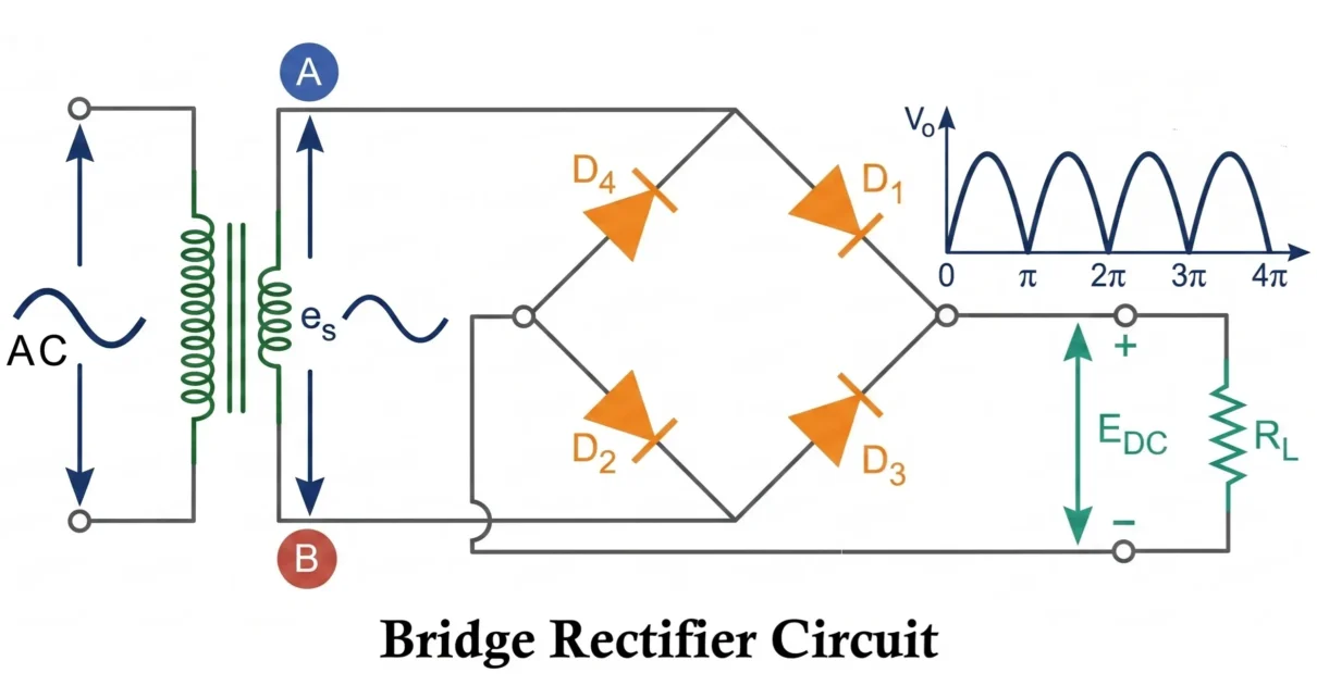
Construction of Bridge Rectifier Circuit
The Bridge Rectifier circuit consists of a step-down transformer (optional), four PN junction diodes arranged in a bridge configuration, a load resistor (RL), and connecting wires. The four diodes are connected in the form of a bridge so that during each half-cycle of the AC input voltage, two diodes conduct while the other two remain reverse biased.
Unlike the Centre-Tap Full-Wave Rectifier, the Bridge Rectifier does not require a center-tapped transformer. This simplifies transformer construction, reduces transformer cost, and improves transformer utilization. The AC input voltage is applied across one diagonal of the bridge, while the load resistance is connected across the other diagonal.

The bridge arrangement automatically directs the current through the load in the same direction during both positive and negative half-cycles of the AC input waveform. As a result, full-wave rectification is achieved without the need for a center tap.
Step-Down Transformer
The transformer is generally used to provide the required AC voltage to the rectifier circuit. Although a Bridge Rectifier can operate directly from an AC source, a transformer is commonly used in practical power supply circuits for safety and voltage adjustment.
The transformer performs the following important functions:
- Provides electrical isolation between the mains supply and the rectifier circuit.
- Steps down the AC voltage to the desired level.
- Improves user safety by isolating the load from the mains supply.
- Supplies the entire secondary voltage to the rectifier during both half-cycles.
Unlike a Centre-Tap Full-Wave Rectifier, the complete secondary winding of the transformer is utilized throughout the entire AC cycle.
The transformer turns ratio is given by:
N2 / N1 = ES / EP
- N1 = Number of primary turns
- N2 = Number of secondary turns
- EP = Primary RMS voltage
- ES = Secondary RMS voltage
The maximum value of the transformer secondary voltage is:
ESM = √2 ES
- ESM = Peak secondary voltage
- ES = RMS secondary voltage
The peak secondary voltage determines the maximum output voltage and Peak Inverse Voltage (PIV) rating of the diodes.
PN Junction Diodes (D1, D2, D3, and D4)
Four PN junction diodes are used as rectifying elements and are connected in the form of a bridge. During each half-cycle of the AC input, two diodes are forward biased and conduct current while the other two are reverse biased and block the current. D1 and D2 conduct during the positive half-cycle, D3 and D4 conduct during the negative half-cycle, and because two diodes conduct at a time, the instantaneous load current is given by:
iL = ESM sin(ωt) / (RL + 2Rf + RS)
- RL = Load resistance
- Rf = Forward resistance of each conducting diode
- RS = Secondary winding resistance of transformer
The term 2Rf appears because two diodes conduct in series during every half-cycle.
Maximum Load Current (Im):
The maximum load current occurs when sin(ωt) = 1.
Im = ESM / (RL + 2Rf + RS)
This current represents the peak value of the rectified load current waveform.
Load Resistance (RL)
The load resistance represents the external device or circuit that consumes the rectified DC power. It may be a resistor, electronic circuit, battery charger, motor drive circuit, or power supply load.
According to Ohm’s Law:
VL = IL × RL
- VL = Load voltage
- IL = Load current
- RL = Load resistance
Because the load receives current during both half-cycles of the AC input waveform, the average DC output voltage and current are significantly higher than those obtained from a Half-Wave Rectifier. The continuous utilization of both half-cycles also results in higher rectification efficiency, lower ripple content, and improved power delivery to the load.
Why Four Diodes are Used in a Bridge Rectifier
The four-diode bridge arrangement eliminates the need for a center-tapped transformer while still achieving full-wave rectification. The bridge automatically switches the current path according to the polarity of the AC input voltage.
This configuration offers several practical advantages:
- No center-tapped transformer is required.
- Lower Peak Inverse Voltage (PIV) requirement per diode.
- Better transformer utilization factor (TUF).
- Higher output power capability.
- Reduced transformer size and cost.
- Widely available as integrated bridge rectifier modules.
These advantages make the Bridge Rectifier the most commonly used rectifier circuit in modern power supply systems, battery chargers, adapters, UPS systems, industrial controllers, and electronic equipment.
Working of Bridge Rectifier Circuit
When an AC voltage is applied to the input terminals of a Bridge Rectifier, the polarity of the applied voltage continuously alternates between positive and negative values. The four diodes arranged in the bridge network automatically switch the current path so that the load current always flows in the same direction.
A Bridge Rectifier Circuit uses four PN junction diodes connected in a bridge configuration. During each half-cycle of the AC input waveform, two diodes conduct while the remaining two diodes remain reverse biased. As the polarity of the AC voltage changes, the conducting pair of diodes also changes automatically.
Although different pairs of diodes conduct during alternate half-cycles, the direction of current through the load remains unchanged. Consequently, both positive and negative half-cycles of the AC input contribute to the load current.
By utilizing the entire AC waveform, the Bridge Rectifier produces a pulsating DC output with higher average DC voltage, improved efficiency, lower ripple content, and better transformer utilization than a Half-Wave Rectifier.
The operation of the circuit is based on the forward and reverse bias characteristics of PN junction diodes and can be understood by analyzing the positive and negative half-cycles separately.
The instantaneous AC voltage applied to the bridge is given by:
es = ESM sin(ωt)
es = Instantaneous secondary voltage
ESM = Peak value of secondary voltage
ω = Angular frequency
t = Time
The angular frequency ω = 2πf, f is the supply frequency.
The relationship between RMS and peak voltage is:
ESM = √2 × ES
ES = ESM / √2
Since the polarity of the AC input voltage reverses every half-cycle, the operation of the Bridge Rectifier is divided into positive and negative half-cycle operation.
Positive Half-Cycle Operation
During the interval 0 ≤ ωt ≤ π, terminal A of the transformer secondary becomes positive with respect to terminal B.
- Diodes D1 and D2 become forward biased.
- Diodes D3 and D4 become reverse biased.
- D1 and D2 conduct current.
- D3 and D4 remain OFF.
- Current flows through the load in the forward direction.

Current Path: Terminal A → D1 → Load Resistance (RL) → D2 → Terminal B
Since two diodes conduct in series, the instantaneous load current is:
iL = es / (RL + 2Rf + RS)
Substituting the value of es:
iL = ESM sin(ωt) / (RL + 2Rf + RS)
Rf = Forward resistance of each conducting diode
RS = Secondary winding resistance
The maximum load current is:
Im = ESM / (RL + 2Rf + RS)
Therefore,
iL = Im sin(ωt)
The load voltage is:
vL = iLRL
vL = ImRL sin(ωt)
During this half-cycle, D1 and D2 behave like closed switches and deliver power to the load.
Negative Half-Cycle Operation
During the interval π ≤ ωt ≤ 2π, the polarity of the AC input voltage reverses. Terminal B becomes positive with respect to terminal A.
- Diodes D3 and D4 become forward biased.
- Diodes D1 and D2 become reverse biased.
- D3 and D4 conduct current.
- D1 and D2 remain OFF.

Current Path: Terminal B → D3 → Load Resistance (RL) → D4 → Terminal A
Although the source polarity has reversed, the current through the load continues to flow in the same direction.
The instantaneous load current is:
iL = -Im sin(ωt)
Since sin(ωt) is negative during this interval, the load current remains positive in direction.
The load voltage is:
vL = |ImRL sin(ωt)|
Thus, power is supplied to the load during both half-cycles of the AC input waveform.
Input and Output Waveforms
The input to the Bridge Rectifier is a sinusoidal AC waveform consisting of positive and negative half-cycles. Due to the bridge arrangement, both half-cycles appear across the load with the same polarity.

Input Waveform:
es = ESM sin(ωt)
- Pure sinusoidal AC waveform.
- Contains positive and negative half-cycles.
- Frequency equal to the supply frequency.
Output Waveform: The output voltage consists of both half-cycles appearing above the zero-reference axis.
- Both positive and negative half-cycles contribute to the output.
- Current through the load remains unidirectional.
- Output voltage always remains positive.
- Average DC output voltage is higher than a Half-Wave Rectifier.
- Ripple content is significantly reduced.
- Power is delivered to the load throughout the complete AC cycle.
The resulting waveform is known as a full-wave pulsating DC waveform. Although its polarity remains constant, its magnitude varies periodically.
Because both halves of the AC waveform are utilized, the ripple frequency doubles, making filtering easier and allowing smaller filter capacitors to be used for obtaining a smooth DC output.
Frequency of Rectifier Output:
Since an output pulse is produced during both half-cycles of the AC input waveform, the output frequency becomes twice the input frequency.
fout = 2fin
- For a 50 Hz AC supply: fout = 100 Hz
- For a 60 Hz AC supply: fout = 120 Hz
This higher ripple frequency is one of the major advantages of the Bridge Rectifier because ripple filtering becomes easier, resulting in a smoother DC output and improved power supply performance.
Performance Analysis of Bridge Rectifier Circuit
The output of a Bridge Rectifier is not a pure DC quantity. Although both half-cycles of the AC input waveform contribute to the output, the resulting waveform still contains alternating components known as ripples. However, the ripple content is much lower than that of a Half-Wave Rectifier, making the output smoother and more suitable for practical DC power supply applications.
Since the Bridge Rectifier utilizes the complete AC waveform, it delivers a higher average DC output voltage, better efficiency, improved transformer utilization, and reduced ripple content compared to a Half-Wave Rectifier.
Various performance parameters are used to evaluate the quality and effectiveness of rectification.
The most important parameters include:
- Average (DC) Load Current
- Average (DC) Output Voltage
- RMS Load Current
- RMS Output Voltage
- Form Factor
- Peak Factor
These parameters form the basis for analyzing the performance of a Bridge Rectifier Circuit and designing efficient AC-to-DC conversion systems.
Average (DC) Load Current (IDC)
The average or DC value of load current represents the useful DC component delivered to the load. Since current flows through the load during both half-cycles of the AC input waveform, the average current is significantly higher than that of a Half-Wave Rectifier.

Mathematically:
For the positive half-cycle:
iL = Im sin(ωt)
For the negative half-cycle:
iL = -Im sin(ωt)
The average value of a periodic waveform is:
IDC = (1 / 2π) ∫ iL d(ωt)
Substituting the full-wave rectified current:
IDC = (1 / π) ∫₀π Im sin(ωt) d(ωt)
Taking Im outside the integral:
IDC = (Im / π) ∫₀π sin(ωt) d(ωt)
Integrating:
IDC = (Im / π) [-cos(ωt)]₀π
IDC = (Im / π) [1 + 1]
IDC = 2Im / π = 0.637 Im
Thus, the average output current is 63.7% of the peak load current.
Peak Load Current (Im):
Since two diodes conduct simultaneously during each half-cycle,
Im = ESM / (RL + 2rf + Rs)
- RL = Load resistance
- rf = Forward resistance of each diode
- Rs = Secondary winding resistance

If diode and transformer resistances are neglected:
Im ≈ ESM / RL
This approximation is commonly used in theoretical calculations.
Average (DC) Output Voltage (VDC)
The DC output voltage is the average voltage developed across the load resistance.
Using Ohm’s Law:
VDC = IDCRL
Substituting IDC:
VDC = (2ImRL) / π
Substituting Im:
VDC = 2ESMRL / [π(RL + 2rf + Rs)]
This is the general expression for the average DC output voltage of a Bridge Rectifier.
Practical Approximation: For most practical circuits RL >> (2rf + Rs)
Therefore,
VDC ≈ 2ESM / π ≈ 0.637 ESM
Thus approximately 63.7% of the peak AC voltage is converted into useful DC voltage.
RMS Value of Load Current (IRMS)
The RMS (Root Mean Square) value represents the equivalent DC current that would produce the same heating effect in the load resistance.
Power calculations are generally based on RMS values.
Mathematically:
IRMS = √[(1 / 2π) ∫ i2L d(ωt)]
Substituting:
IRMS = √[(1 / 2π) ∫₀²π I2m sin2(ωt) d(ωt)]
Taking I2m outside:
IRMS = Im √[(1 / 2π) ∫₀²π sin2(ωt) d(ωt)]
Using the trigonometric identity:
sin2(ωt) = (1 − cos2ωt)/2
After integration:
IRMS = Im / √2 = 0.707 Im
The RMS current is considerably higher than that of a Half-Wave Rectifier because current flows throughout the complete AC cycle.
RMS Value of Output Voltage (VRMS)
The RMS output voltage is obtained from the RMS current flowing through the load.
Using Ohm’s Law:
VRMS = IRMSRL
Substituting IRMS:
VRMS = (ImRL) / √2
Substituting Im:
VRMS = ESMRL / [√2(RL + 2rf + Rs)]
For an ideal Bridge Rectifier:
VRMS ≈ ESM / √2
Relationship Between Peak, RMS, and Average Values of a Bridge Rectifier
| Parameter | Expression | Numerical Value |
|---|---|---|
| Peak Current | Im | 1.0 Im |
| Average Current | 2Im/π | 0.637 Im |
| RMS Current | Im/√2 | 0.707 Im |
| Peak Voltage | ESM | 1.0 ESM |
| Average Voltage | 2ESM/π | 0.637 ESM |
| RMS Voltage | ESM/√2 | 0.707 ESM |
These relationships are extensively used in bridge rectifier design and performance calculations.
Form Factor
Form Factor is defined as the ratio of RMS value to the average value of the output waveform.
Form Factor = RMS Value / Average Value
For a Bridge Rectifier:
Form Factor = IRMS / IDC
Substituting the values:
Form Factor = (Im/√2) / (2Im/π)
Form Factor = π / 2√2
Form Factor = 1.11
A pure DC waveform has a Form Factor of 1, while a Bridge Rectifier has a Form Factor of 1.11. This value is very close to unity, indicating that the output waveform contains relatively small AC variations and more closely resembles pure DC than the output of a Half-Wave Rectifier.
Peak Factor (Crest Factor)
The Peak Factor indicates the ratio of the peak value of a waveform to its RMS value. It is an important parameter in rectifier design because it helps determine the maximum current and voltage stresses experienced by diodes, transformers, filter capacitors, and other power supply components.
Peak Factor = Peak Value / RMS Value
For load current:
Peak Factor = Im / IRMS
Substituting:
Peak Factor = Im / (Im/√2) = √2
Peak Factor = 1.414
The Peak Factor of a Bridge Rectifier is significantly lower than that of a Half-Wave Rectifier, indicating a smoother output waveform and reduced peak current stress. This parameter is particularly important when selecting filter capacitors, transformers, diodes, and voltage regulators that must withstand transient current peaks.
DC Power Output (PDC)
The primary objective of a Bridge Rectifier is to convert AC electrical power into useful DC power. The DC power output represents the useful power delivered to the load resistance by the DC component of the rectified output.
Since the load utilizes the average component of the rectified waveform, the DC output power is calculated using the average load current.
Mathematical Expression:
The DC output power is:
PDC = IDC2RL
Substituting:
IDC = 2Im/π
we obtain:
PDC = (2Im/π)2RL
Therefore,
PDC = 4Im2RL/π2
Since 4/π2 = 0.405,
PDC = 0.405 Im2RL
This represents the useful DC power delivered to the load. Since both half-cycles of the AC input contribute to the output, the DC power obtained from a Bridge Rectifier is substantially greater than that of a Half-Wave Rectifier operating under identical conditions.
AC Power Input (PAC)
The AC power supplied by the transformer secondary is consumed by:
- Load resistance (RL)
- Forward resistance of the conducting diodes (2rf)
- Transformer secondary winding resistance (Rs)
Unlike a Centre-Tap Full-Wave Rectifier, two diodes conduct simultaneously in every half-cycle. Therefore, the forward resistance contribution becomes 2rf.
Mathematical Expression:
The AC input power is:
PAC = IRMS2(RL + 2rf + Rs)
Substituting:
IRMS = Im/√2
PAC = (Im/√2)2(RL + 2rf + Rs)
PAC = Im2/2 × (RL + 2rf + Rs)
PAC = 0.5 Im2(RL + 2rf + Rs)
This represents the total power drawn from the AC source. A portion of this power is delivered to the load, while the remainder is dissipated as heat in the diodes and transformer winding resistance.
Rectification Efficiency (η)
Rectification Efficiency indicates how effectively a Bridge Rectifier converts AC input power into useful DC output power.
It is defined as the ratio of DC power delivered to the load to the AC power supplied by the source.
Mathematically:
η = PDC / PAC
Substituting the expressions for PDC and PAC:
η = [4Im2RL/π2] / [(Im2/2)(RL + 2rf + Rs)]
Cancelling Im2:
η = 8RL / [π2(RL + 2rf + Rs)]
Since 8/π2 = 0.812, the efficiency becomes
η = 0.812 RL / (RL + 2rf + Rs)
η = 0.812 / [1 + (2rf + Rs)/RL]
Percentage Efficiency:
η(%) = 81.2 / [1 + (2rf + Rs)/RL]
Maximum Rectification Efficiency: For an ideal Bridge Rectifier rf = 0 and Rs = 0.
ηmax = 81.2%
Thus, under ideal conditions, a maximum of 81.2% of the AC input power is converted into useful DC output power.
Why Bridge Rectifier Efficiency is High?
- Both half-cycles of the AC input waveform are utilized.
- Power is delivered to the load throughout the entire AC cycle.
- The complete transformer secondary winding is utilized.
- Ripple content is significantly reduced.
- More input power is converted into useful DC output.
As a result, Bridge Rectifiers are extensively used in power adapters, battery chargers, industrial power supplies, UPS systems, and electronic equipment.
Ripple Factor (γ)
Although the Bridge Rectifier produces a smoother output than a Half-Wave Rectifier, some AC components still remain superimposed on the DC output. These unwanted AC components are known as ripples.
Ripples are responsible for:
- Output voltage fluctuations.
- Noise in electronic circuits.
- Reduced power quality.
- Deviation from ideal DC output.
The amount of ripple present in the output is measured using Ripple Factor.
Ripple Factor is defined as the ratio of the RMS value of the AC component to the DC component of the output.
γ = IAC / IDC
The output current contains both AC and DC components.
IRMS2 = IDC2 + IAC2
Rearranging:
IAC2 = IRMS2 − IDC2
Taking square root:
IAC = √(IRMS2 − IDC2)
Substituting into the Ripple Factor equation:
γ = √[(IRMS/IDC)2 − 1]
Substituting: IRMS = Im/√2 and IDC = 2Im/π,
γ = √[(π/2√2)2 − 1]
γ = √(1.234 − 1)
γ = √0.234 = 0.482
Ripple Factor = 0.482
This means the AC ripple component is only 48.2% of the DC component. Compared with the Ripple Factor of 1.21 for a Half-Wave Rectifier, the Bridge Rectifier produces a much smoother DC output and requires less filtering.
Ripple Factor and Output Quality:
- Smaller Ripple Factor: Better DC output, reduced fluctuations, easier filtering, and improved performance.
- Larger Ripple Factor: Poor DC output, increased noise, larger voltage variations, and higher filtering requirements.
For a pure DC source, γ = 0. Since the bridge rectifier has γ = 0.482, its output is much closer to ideal DC than the output of a half-wave rectifier.
Fourier Analysis of Bridge Rectifier Output
The pulsating output of a Bridge Rectifier can be represented as the sum of a DC component and several AC harmonic components. This analysis is based on Fourier Series.
Like the Centre-Tap Full-Wave Rectifier, the Bridge Rectifier utilizes both half-cycles of the input AC waveform. Consequently, the output contains a larger DC component, lower ripple content, and harmonic components that begin at twice the supply frequency.
Fourier Series Representation: The load current can be expressed as:
iL = IDC + Harmonic Components
The Fourier Series of the full-wave rectified current is:
iL = (2Im/π) − (4Im/π)[cos(2ωt)/3 + cos(4ωt)/15 + cos(6ωt)/35 + ...]
The first term represents the DC component, while the remaining terms represent the ripple components.
Components Present in Output: The complete output waveform consists of a DC component and even harmonic components.
DC Component: This is the useful output current delivered to the load.
IDC = 2Im/π
Lowest Ripple Frequency: The lowest AC component present in the output occurs at 2f, f is the supply frequency.
- For a 50 Hz supply, lowest ripple frequency = 100 Hz
- For a 60 Hz supply, lowest ripple frequency = 120 Hz
Harmonic Components: Additional frequency components occur at 2f, 4f, 6f, 8f, …. These harmonic components contribute to ripple and waveform distortion.
Because the ripple frequency is twice the supply frequency, filtering is considerably easier than in a Half-Wave Rectifier. As a result, smaller filter capacitors can be used to achieve a smooth DC output.
Fourier analysis helps to:
- Design filter circuits.
- Estimate ripple content.
- Analyze harmonic distortion.
- Improve power supply performance.
- Select appropriate smoothing capacitors.
It clearly shows that the output of a Bridge Rectifier is not pure DC but a combination of a large DC component and relatively small AC harmonic components. Since the Bridge Rectifier produces the same output waveform as a Centre-Tap Full-Wave Rectifier, both have identical Fourier components, ripple frequency, and ripple factor characteristics.
Peak Inverse Voltage (PIV)
Peak Inverse Voltage (PIV) is the maximum reverse voltage that a diode can withstand safely without entering the breakdown region.
The PIV rating is one of the most important parameters when selecting diodes for a Bridge Rectifier because excessive reverse voltage can permanently damage the diode junction.
Unlike a Centre-Tap Full-Wave Rectifier, where the non-conducting diode must withstand twice the peak secondary voltage, the reverse voltage in a Bridge Rectifier is shared by the bridge configuration.
PIV in Bridge Rectifier: During each half-cycle, two diodes conduct while the other two remain reverse-biased, with the reverse voltage distributed across the bridge network.
The maximum reverse voltage across each diode is:
PIV = ESM
Since ESM = √2ES,
PIV = √2ES
Example: If the transformer secondary voltage ES = 12 V RMS
PIV = 1.414 × 12
PIV = 16.97 V
Therefore, a diode with a reverse voltage rating greater than 16.97 V should be selected. In practice, a safety factor of 2 to 3 is normally used.
Advantages of Lower PIV Requirement:
- Lower-cost diodes can be used.
- Improved reliability.
- Reduced risk of reverse breakdown.
- Better suitability for high-voltage applications.
The lower PIV requirement is one of the major advantages of a Bridge Rectifier over a Centre-Tap Full-Wave Rectifier, where each diode must withstand twice the peak secondary voltage.
Transformer Utilization Factor (TUF)
The transformer is one of the most expensive and important components in a rectifier circuit. Therefore, it is essential to determine how effectively the transformer rating is utilized in delivering useful DC power to the load.
This effectiveness is measured using the Transformer Utilization Factor (TUF).
Transformer Utilization Factor is defined as the ratio of DC power delivered to the load to the AC rating of the transformer.
TUF = DC Power Delivered to Load / AC Rating of Transformer
A higher TUF indicates better utilization of transformer copper, magnetic core material, and transformer VA rating.
For a Bridge Rectifier:
TUF = 0.812
This means approximately:
81.2%
of the transformer rating is effectively utilized.
This value is higher than:
- Half-Wave Rectifier: TUF = 0.287
- Centre-Tap Full-Wave Rectifier: TUF = 0.693
Why TUF is Highest in a Bridge Rectifier?
- The entire transformer secondary winding is utilized during both half-cycles.
- Current flows through the transformer throughout the complete AC cycle.
- No center-tapped transformer is required.
- Transformer copper utilization is improved.
- Transformer core utilization is maximized.
- DC power output is higher for a given transformer rating.
A higher TUF results in:
- Better transformer utilization.
- Higher power output capability.
- Smaller transformer size for the same DC output power.
- Reduced transformer cost.
- Improved overall system efficiency.
This excellent transformer utilization is one of the primary reasons why Bridge Rectifiers are preferred in modern power supply designs.
Voltage Regulation
An ideal rectifier should maintain a constant output voltage regardless of variations in load current. In practical Bridge Rectifiers, however, the output voltage decreases as the load current increases because of voltage drops across the transformer winding resistance and conducting diodes.
This behavior is measured using Voltage Regulation.
Voltage Regulation indicates the change in output voltage as the load changes from no-load condition to full-load condition.
Formula of Voltage Regulation:
Voltage Regulation (%) = [(VNL − VFL) / VFL] × 100
- VNL = No-load output voltage
- VFL = Full-load output voltage
No-Load Condition: Under no-load condition RL → ∞
The load current becomes approximately zero.
- Voltage drop across the conducting diodes becomes negligible.
- Voltage drop across transformer winding resistance becomes negligible.
- The output voltage reaches its maximum value.
VNL ≈ 2ESM/π
Full-Load Condition: Under full-load conditions, the load current increases, causing larger voltage drops across the transformer winding resistance Rs and the two conducting diode resistances 2rf.
Therefore, VFL < VNL, and the DC output voltage is:
VDC = 2ESMRL / [π(RL + 2rf + Rs)]
At full load:
VFL = 2ESMRL / [π(RL + 2rf + Rs)]
Substituting into the voltage regulation equation and simplifying:
Voltage Regulation (%) = (2rf + Rs) / RL × 100
Ideal Voltage Regulation: For an ideal Bridge Rectifier rf = 0 and Rs = 0
Voltage Regulation = 0%
This indicates a perfectly constant output voltage independent of load current.
Significance of Voltage Regulation:
- Low Regulation
- Stable output voltage.
- Better load handling capability.
- Improved power supply performance.
- Higher quality DC output.
- High Regulation
- Large output voltage variations.
- Poor load regulation.
- Reduced power supply stability.
For a well-designed Bridge Rectifier power supply, voltage regulation should be as low as possible.
Regulation Characteristics
The relationship between output voltage and load current is represented by the Regulation Characteristic Curve.
As load current increases, the voltage drops across the transformer winding resistance and conducting diodes increase, causing the output voltage to decrease.

Output Voltage ∝ 1 / Load Current
The resulting characteristic is a downward-sloping curve.
Applying Kirchhoff’s Voltage Law:
ESM = ILRs + 2ILrf + VL
Rearranging:
VL = ESM − IL(Rs + 2rf)
This equation clearly shows that as load current increases, the output voltage decreases, producing the characteristic drooping regulation curve of a Bridge Rectifier.
Design Considerations for Bridge Rectifier Circuit
When designing a Bridge Rectifier, several practical factors must be considered to ensure reliable operation, maximum efficiency, and long component life.
- Diode Selection
- Forward current rating must exceed the maximum load current.
- PIV rating must be greater than the peak secondary voltage.
- Low forward voltage drop diodes improve efficiency.
- Fast recovery diodes are preferred for high-frequency applications.
- A suitable safety margin should be included for transient voltages.
- Transformer Selection
- Required DC output voltage.
- Required load current.
- Transformer VA rating.
- Isolation and safety requirements.
- Voltage drop due to two conducting diodes.
- Load Resistance RL
- Determines load current.
- Affects output voltage.
- Influences efficiency and regulation.
- Controls power delivered to the load.
- Heat Dissipation
- Power is dissipated in two conducting diodes during each half-cycle.
- Transformer winding resistance also generates heat.
- High-current applications may require heat sinks.
- Proper thermal management improves reliability and lifespan.
- Filtering Requirements
- The ripple factor of a Bridge Rectifier is γ = 0.482.
- Ripple is significantly lower than that of a Half-Wave Rectifier.
- Filters are commonly used to obtain smoother DC output.
- Common filters include Capacitor Filters, Inductor Filters, LC Filters, and Pi Filters.
- These filters further reduce ripple voltage and improve power quality.
Bridge Rectifier Circuit with Capacitor Filter
Although the Bridge Rectifier produces a full-wave rectified output, some ripple voltage still remains. To obtain a smoother DC output, a filter circuit is connected between the rectifier and the load.
The capacitor filter is the most commonly used filtering method because it is simple, inexpensive, and highly effective.
A capacitor connected across the load charges to the peak rectifier voltage and discharges slowly through the load resistance when the rectifier voltage falls below the capacitor voltage.
This charging and discharging action helps maintain a nearly constant DC output voltage.
During the Positive Half-Cycle
- Diodes D1 and D2 conduct.
- The capacitor charges rapidly.
- The capacitor voltage rises nearly to the peak rectified voltage.
- The load receives current directly from the rectifier.
The capacitor charges approximately to:
VC ≈ ESM
VC = Capacitor voltage
During the Negative Half-Cycle
- Diodes D3 and D4 conduct.
- A fresh charging pulse is applied to the capacitor.
- The capacitor is recharged before significant discharge occurs.
- The load receives nearly continuous current.
Between charging intervals, the capacitor discharges through the load.
The capacitor discharge voltage is:
VC = V0e-t/(RLC)
- V0 = Initial capacitor voltage
- RL = Load resistance
- C = Filter capacitance
- t = Time
Effects of the Capacitor Filter
Because the capacitor discharges slowly, the output voltage remains nearly constant and ripple voltage is greatly reduced.
Capacitor Filter Benefits:
- Increases average output voltage.
- Reduces ripple factor.
- Improves voltage regulation.
- Produces smoother DC output.
- Reduces output voltage fluctuations.
- Improves overall power supply performance.
However, excessively large capacitors increase charging current, diode peak-current stress, transformer loading, size, and cost. Therefore, the capacitor value should be selected carefully based on load current and permissible ripple voltage.
Ripple Frequency:
For a Bridge Rectifier:
fr = 2f
- fr = Ripple frequency
- f = Supply frequency (50 Hz or 60 Hz)
Since the ripple frequency is twice the supply frequency, filtering is much easier than in a Half-Wave Rectifier and requires a smaller filter capacitor to achieve the same level of smoothing.
Approximate Ripple Voltage
For a capacitor-filtered Bridge Rectifier:
Vr(pp) ≈ IDC / (2fC)
- Vr(pp) = Peak-to-peak ripple voltage
- IDC = DC load current
- f = Supply frequency
- C = Filter capacitance
This equation shows that ripple voltage decreases as capacitance and ripple frequency increase, and as load current decreases.
For this reason, Bridge Rectifiers with capacitor filters are extensively used in DC power supplies, battery chargers, adapters, UPS systems, industrial controllers, and electronic power conversion equipment.
Advantages of Bridge Rectifier Circuit
- No Center-Tapped Transformer Required: The Bridge Rectifier operates with a standard transformer, simplifying construction and reducing cost.
- Higher Rectification Efficiency: The maximum theoretical rectification efficiency is ηmax = 81.2%, allowing more input AC power to be converted into useful DC power.
- Utilizes Both Half-Cycles of AC Input: Both positive and negative half-cycles contribute to the output, providing full utilization of the input waveform.
- Higher Average DC Output Voltage: The average DC output voltage is significantly higher than that of a Half-Wave Rectifier.
- Lower Ripple Content: The ripple factor is γ = 0.482, producing a smoother DC output than a Half-Wave Rectifier.
- Higher Ripple Frequency: The ripple frequency is twice the supply frequency (2f), making filtering easier and reducing filter size requirements.
- Better Transformer Utilization: The Transformer Utilization Factor (TUF) is 0.812, which is higher than that of a Centre-Tap Full-Wave Rectifier, resulting in more effective use of the transformer.
- Lower Peak Inverse Voltage Requirement: Each diode requires a PIV rating of only ESM, reducing diode voltage-rating requirements and cost.
- Improved Output Quality: Continuous power delivery during both half-cycles reduces output fluctuations and improves DC quality.
- No DC Saturation of Transformer Core: Alternating secondary current prevents DC magnetization and minimizes core saturation effects.
- Compact and Economical Design: The absence of a center tap and improved transformer utilization often allow smaller transformers and lower overall system cost.
- Available as Integrated Modules: Bridge rectifier modules containing four diodes in a single package simplify assembly and improve reliability.
- Suitable for Medium- and High-Power Applications: High efficiency, good transformer utilization, and low ripple make the Bridge Rectifier suitable for power supply applications.
Disadvantages of Bridge Rectifier Circuit
- Requires Four Diodes: The circuit uses four diodes compared to one diode in a Half-Wave Rectifier and two diodes in a Centre-Tap Full-Wave Rectifier, increasing component count.
- Higher Forward Voltage Drop: During each half-cycle, current passes through two diodes connected in series. Therefore, the total forward voltage drop is approximately twice that of a Centre-Tap Full-Wave Rectifier.
- Reduced Output Voltage in Low-Voltage Applications: The voltage drop across two conducting diodes can significantly reduce the output voltage in low-voltage power supply circuits.
- Higher Power Dissipation in Diodes: Since two diodes conduct simultaneously, power loss in the rectifier section is greater than that of a Centre-Tap Full-Wave Rectifier.
- Heat Generation: Additional power dissipation produces heat, which may require heat sinks in high-current applications.
- More Complex than Half-Wave Rectifier: The bridge configuration requires additional components and wiring, making the circuit slightly more complex.
- Not Suitable for Extremely Low Voltage Outputs: In low-voltage power supplies, the combined forward voltage drop of two diodes can become a significant percentage of the total output voltage.
Applications of Bridge Rectifier Circuit
- Linear DC Power Supplies: Widely used in regulated and unregulated power supply circuits to convert AC voltage into DC voltage.
- Battery Charging Circuits: Commonly used in battery chargers due to its high efficiency and smooth DC output.
- AC to DC Power Adapters: Used in mobile chargers, laptop adapters, routers, set-top boxes, and consumer electronic equipment.
- Audio Amplifier Power Supplies: Provides stable DC voltage with reduced ripple and lower hum levels.
- Laboratory Power Supplies: Used extensively in laboratory and educational power supply units.
- Industrial Control Systems: Supplies DC power for PLCs, relays, contactors, sensors, timers, and automation equipment.
- UPS Systems: Used in Uninterruptible Power Supply systems for AC-to-DC conversion stages.
- SMPS Front-End Rectification: Used as the input rectification stage in many Switch Mode Power Supplies (SMPS).
- DC Motor Drives: Used in low-power DC motor control and drive applications.
- Instrumentation Systems: Suitable for measurement and monitoring equipment requiring stable DC power.
- Communication Equipment: Used in radio communication, networking equipment, and telecommunication systems.
- Embedded and Microcontroller Systems: Serves as the front-end AC-to-DC conversion stage for embedded electronics.
- LED Driver Power Supplies: Used in LED lighting systems requiring DC power derived from AC mains.
- General Purpose AC-to-DC Conversion: Used wherever reliable and efficient DC power generation from AC sources is required.
Bridge Rectifier vs Centre-Tap Full-Wave Rectifier
The following comparison highlights the differences between a Bridge Rectifier and a Centre-Tap Full-Wave Rectifier.
| Parameter | Centre-Tap Full-Wave Rectifier | Bridge Rectifier |
|---|---|---|
| Number of Diodes | 2 | 4 |
| Transformer Requirement | Center-Tapped Transformer | Ordinary Transformer |
| Center Tap Required | Yes | No |
| Utilization of Input Cycle | 100% | 100% |
| Average Output Voltage | 0.637 ESM | 0.637 ESM |
| Average Output Current | 0.637 Im | 0.637 Im |
| Ripple Factor | 0.482 | 0.482 |
| Form Factor | 1.11 | 1.11 |
| Maximum Efficiency | 81.2% | 81.2% |
| Ripple Frequency | 2f | 2f |
| PIV per Diode | 2ESM | ESM |
| Transformer Utilization Factor | 0.693 | 0.812 |
| Diodes Conducting per Half-Cycle | 1 | 2 |
| Forward Voltage Drop | One Diode Drop | Two Diode Drops |
| Transformer Cost | Higher | Lower |
| Transformer Size | Larger | Smaller |
| Circuit Complexity | Moderate | Moderate |
| Power Handling Capability | Medium | High |
| Industrial Usage | Less Common | Most Widely Used |
The comparison clearly shows that the Bridge Rectifier offers superior transformer utilization, lower PIV requirements, reduced transformer cost, and easier transformer design. Although it requires four diodes and introduces an additional diode voltage drop, it remains the most widely used rectifier circuit in modern AC-to-DC power conversion systems.
Practical Design Example
Consider a Bridge Rectifier Circuit with the following specifications:
- Transformer Secondary Voltage: 12 V RMS
- Load Resistance (RL): 1 kΩ
- Diode Forward Voltage Drop (VD): 0.7 V per diode
- Diode Forward Resistance (rf): 20 Ω per diode
- Transformer Secondary Resistance (Rs): 10 Ω
Peak Secondary Voltage
ESM = √2 × ES
ESM = 1.414 × 12 = 16.97 V
Total Series Resistance
Since two diodes conduct simultaneously in a Bridge Rectifier,
R = RL + 2rf + Rs
R = 1000 + (2 × 20) + 10
R = 1050 Ω
Peak Current
Since current flows through two conducting diodes,
Im = (ESM − 2VD) / R
Im = (16.97 − 1.4) / 1050
Im = 14.83 mA
Average DC Current
For a Bridge Rectifier:
IDC = 2Im/π
IDC = (2 × 14.83)/π
IDC = 9.44 mA
Average DC Output Voltage
VDC = IDC × RL
VDC = 9.44 × 1000
VDC = 9.44 V
RMS Current
IRMS = Im/√2
IRMS = 14.83/1.414
IRMS = 10.49 mA
Diode PIV Rating
For a Bridge Rectifier:
PIV = ESM
PIV = 16.97 V
In practice, a diode with a significantly higher PIV rating (e.g., 50 V, 100 V, or greater) should be selected to provide a suitable safety margin against voltage surges and transient conditions.
Rectification Efficiency
For practical circuits:
η = 0.812 RL / (RL + 2rf + Rs)
η = 0.812 × 1000 / 1050
η = 0.773
η = 77.3%
Final Results
- Peak Secondary Voltage: 16.97 V
- Peak Current: 14.83 mA
- Average DC Current: 9.44 mA
- Average DC Output Voltage: 9.44 V
- RMS Current: 10.49 mA
- Rectification Efficiency: 77.3%
- Required PIV Rating: ≥ 16.97 V
This example illustrates a practical Bridge Rectifier design by considering diode forward voltage drops, forward resistance, transformer winding resistance, rectification efficiency, and diode PIV requirements.
Conclusion
The Bridge Rectifier is one of the most widely used AC-to-DC conversion circuits in modern electronics and power supply systems. By utilizing both half-cycles of the AC input waveform, it delivers a higher average DC output voltage, superior transformer utilization, lower ripple content, and significantly better efficiency than a Half-Wave Rectifier.
Unlike the Centre-Tap Full-Wave Rectifier, the Bridge Rectifier does not require a center-tapped transformer and offers a lower Peak Inverse Voltage (PIV) requirement for each diode. These advantages make it the preferred choice for power adapters, battery chargers, industrial power supplies, communication systems, and electronic equipment.
Key Takeaways
- Bridge Rectifier: Uses four diodes connected in a bridge configuration to convert AC into pulsating DC.
- Rectification Principle: Two diodes conduct during each half-cycle, ensuring current always flows through the load in the same direction.
- Maximum Rectification Efficiency: ηmax = 81.2%
- Ripple Factor: γ = 0.482, indicating much lower ripple than a Half-Wave Rectifier.
- Transformer Utilization Factor: TUF = 0.812, providing better transformer utilization than a Centre-Tap Full-Wave Rectifier.
- Peak Inverse Voltage: PIV = ESM = √2ES
- Ripple Frequency: fr = 2f
- No Center-Tapped Transformer Required: Can operate using a standard transformer.
- Filtering: Capacitor filters are commonly used to further reduce ripple and improve output smoothness.
- Applications: Widely used in DC power supplies, battery chargers, industrial electronics, communication systems, UPS systems, and power adapters.
- Importance: Forms the foundation for understanding AC-to-DC power conversion, filter circuits, voltage regulators, and modern power supply design.
Important Equations
- Current Equations
- Im = ESM / (RL + 2rf + Rs)
- IDC = 2Im / π
- IRMS = Im / √2
- Voltage Equations
- VDC = 2ESMRL / [π(RL + 2rf + Rs)]
- VDC ≈ 2ESM / π (Ideal Diodes)
- VRMS = ESMRL / [√2(RL + 2rf + Rs)]
- VRMS ≈ ESM / √2 (Ideal Diodes)
- Power Equations
- PDC = IDC2RL
- PAC = IRMS2(RL + 2rf + Rs)
- Performance Parameters
- Form Factor = 1.11
- Peak Factor = 1.414
- η = 0.812 × RL / (RL + 2rf + Rs)
- ηmax = 81.2%
- γ = √[(IRMS/IDC)² − 1] = 0.482
- TUF = 0.812
- PIV = ESM
- Voltage Regulation (%) = [(VNL − VFL) / VFL] × 100
The Bridge Rectifier remains the most widely used rectifier circuit because it offers an excellent combination of simplicity, efficiency, low ripple, lower PIV requirements, and superior transformer utilization. Understanding its operation and performance characteristics provides a strong foundation for advanced power electronics, power conversion systems, and modern DC power supply design.
Frequently Asked Questions (FAQs)
- What is a Bridge Rectifier? A full-wave rectifier circuit that uses four diodes arranged in a bridge configuration to convert AC into pulsating DC.
- Why is it called a Bridge Rectifier? Because the four diodes are connected in the form of an electrical bridge.
- How many diodes are required? Four.
- Does it require a center-tapped transformer? No, it can operate with a standard transformer.
- What is the output waveform? Full-wave pulsating DC.
- What is the ripple factor? γ = 0.482.
- What is the maximum efficiency? ηmax = 81.2%.
- What is the Peak Inverse Voltage (PIV)? PIV = ESM.
- What is the Transformer Utilization Factor (TUF)? TUF = 0.812.
- What is the ripple frequency? fr = 2f.
- Can it produce pure DC? No, filtering is still required.
- Which filter is commonly used? Capacitor filter.
- What is the major advantage? No center-tapped transformer is required and transformer utilization is excellent.
- Why is it more efficient than a Half-Wave Rectifier? Because it utilizes both half-cycles of the AC input waveform.
- Where is it commonly used? Power supplies, battery chargers, UPS systems, industrial electronics, communication equipment, adapters, and consumer electronic products.
Quick Interview Questions
- What is a Bridge Rectifier?
- Why are four diodes used in a Bridge Rectifier?
- Explain operation during positive and negative half-cycles.
- Why does current through the load remain unidirectional?
- What is full-wave rectification?
- Define PIV, ripple factor, TUF, and voltage regulation.
- Derive IDC, IRMS, and VDC.
- Derive rectification efficiency and ripple factor.
- Compare Bridge Rectifier and Centre-Tap Full-Wave Rectifier.
- Why is the ripple frequency equal to twice the supply frequency?
- Explain the effect of a capacitor filter.
- Why is transformer utilization higher in a Bridge Rectifier?
- Why is the PIV requirement lower than that of a Centre-Tap Full-Wave Rectifier?
Rectifier Circuit: Construction, Working, Types and Applications
Centre-Tap Full-Wave Rectifier Circuit Design and Performance Analysis
Types of Diodes: Symbol, Working, Characteristics and Applications
Diode Clipper Circuit Diagram, Types, Working and Applications
Diode Clamper Circuit Diagram, Types, Working and Applications
Light Emitting Diode LED – Symbol, Construction, Working, Types and Applications
