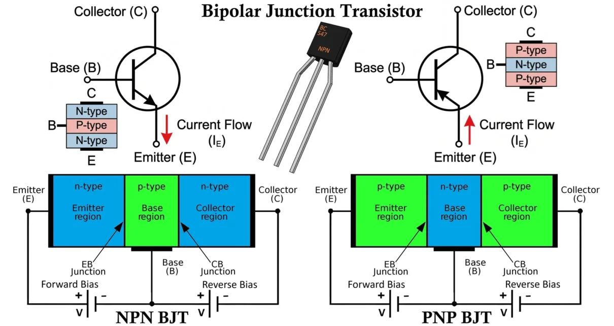
Bipolar Junction Transistors (BJTs) are widely used semiconductor devices for amplification and switching applications. A BJT consists of three layers of doped semiconductor material that form two PN junctions. These three regions are known as the Emitter, Base, and Collector. NPN and PNP are the two main types of Bipolar Junction Transistors.
Unlike Field Effect Transistors (FETs), which use only one type of charge carrier, BJTs use both electrons and holes for current conduction. Because of their excellent current amplification and switching characteristics, BJTs are widely used in analog electronics, digital circuits, power supplies, communication systems, industrial automation, and countless other electronic applications.
Why is it Called a Bipolar Junction Transistor (BJT)?
The name Bipolar Junction Transistor (BJT) describes both the construction and operating principle of the device.

Bipolar means there are two types of charge carriers, electrons and holes participating in current conduction. Unlike Field Effect Transistors (FETs), which rely on only one type of charge carrier, a BJT uses both majority and minority carriers to control current flow, making it a bipolar semiconductor device.
The term Junction refers to the two PN junctions formed within the transistor. One junction exists between the emitter and base, while the other is located between the collector and base. Proper biasing of these two junctions allows the transistor to operate as an amplifier or an electronic switch.
The word Transistor is derived from the combination of two words:
TRANSfer + resISTOR = TRANSISTOR
The name reflects the transistor’s ability to transfer a signal from a low-resistance input circuit to a high-resistance output circuit while providing amplification. A small current applied to the base controls a much larger current flowing between the collector and emitter.
Related Articles:
- MOSFET: Metal Oxide Semiconductor Field Effect Transistor
- JFET Junction Field Effect Transistors Working and Applications
- IGBT Full Form, Symbol, Construction, Working and Applications
- UJT Unijunction Transistor Symbol, Construction & Working
- Difference Between Photodiode, Phototransistor and Photoresistor
- Types of Transistors: Classification (BJT, JFET, MOSFET & IGBT)
Symbol of Bipolar Junction Transistors (BJTs)
The symbol of a Bipolar Junction Transistor varies depending on whether it is an NPN or PNP transistor.

- NPN Transistor: The arrow on the emitter points outward.
- PNP Transistor: The arrow on the emitter points inward.
Based on the arrangement of P-type and N-type semiconductor materials, Bipolar Junction Transistors can be NPN or PNP.
Both transistor types operate on the same fundamental principle but differ in the arrangement of semiconductor layers, the majority charge carriers, and the direction of current flow.
Construction of Bipolar Junction Transistor (BJT)
A Bipolar Junction Transistor (BJT) is a three-terminal semiconductor device made from three layers of semiconductor material, forming two PN junctions. Depending on the arrangement of the semiconductor layers, BJTs are manufactured as either NPN or PNP transistors.
The three semiconductor regions are Emitter (E), Base (B) and Collector (C)
Each region has a different doping concentration and performs a specific function during transistor operation.
Emitter, Base, and Collector Explained
The following table summarizes the construction and function of each transistor region.
| Region | Doping Level | Main Function |
|---|---|---|
| Emitter (E) | Heavily Doped | Injects a large number of charge carriers into the base. |
| Base (B) | Very Thin & Lightly Doped | Controls the flow of charge carriers between the emitter and collector. |
| Collector (C) | Moderately Doped | Collects charge carriers and dissipates the generated heat. |
Emitter (E)
The emitter is designed to inject a large number of electrons (in an NPN transistor) or holes (in a PNP transistor) into the base region. Since carrier injection is its primary function, the emitter is heavily doped to maximize carrier concentration and improve transistor efficiency.
Base (B)
The base is the thinnest region of the transistor and is lightly doped. Its primary purpose is to regulate the collector current. Because the base is extremely thin, only a small percentage of injected carriers recombine within it, while the majority continue toward the collector.
This unique construction allows a very small base current to control a much larger collector current, resulting in current amplification.
Collector (C)
The collector receives most of the charge carriers emitted by the emitter after they pass through the base region. It is physically larger than the emitter because it must withstand higher voltages, dissipate more heat, and handle greater power during operation.
Construction of NPN and PNP Transistors
NPN Transistor
An NPN transistor consists of a thin P-type semiconductor layer sandwiched between two N-type semiconductor regions.

Emitter (E):
- Heavily doped with N-type material.
- Emits electrons into the base.
Base (B):
- Thin and lightly doped with P-type material.
- Controls the number of electrons passing through.
Collector (C):
- Moderately doped with N-type material.
- Collects electrons from the base.
PNP Transistor
A PNP transistor consists of a thin N-type semiconductor layer placed between two P-type semiconductor regions.

Emitter (E):
- Heavily doped with P-type material.
- Emits holes into the base.
Base (B):
- Thin and lightly doped with N-type material.
- Controls the number of holes passing through.
Collector (C):
- Moderately doped with P-type material.
- Collects holes from the base.
Physical Structure
- Layers: In both NPN and PNP transistors, the layers are arranged in the sequence of emitter, base, and collector.
- Doping Levels: The emitter is heavily doped to inject a high number of charge carriers. The base is thin and lightly doped to allow most carriers to pass through to the collector. The collector is moderately doped and larger in size to collect the carriers.
PN Junctions in Bipolar Junction Transistor
A Bipolar Junction Transistor contains two PN junctions that work together to control current flow.
- Emitter-Base Junction (EB Junction): Formed between the emitter and base.
- Collector-Base Junction (CB Junction): Formed between the collector and base.
During normal active-mode operation, the emitter-base junction is forward biased while the collector-base junction is reverse biased. This biasing arrangement allows charge carriers injected by the emitter to move through the thin base region and reach the collector with very little recombination.
Unbiased PN Junction: Depletion Region and Barrier Potential
The movement of these carriers enables the transistor to amplify current efficiently, making the BJT suitable for amplification and switching applications.
Why is the Collector Larger than the Emitter?
One of the most common questions asked in transistor theory is why the collector region is physically larger than the emitter. The answer lies in heat dissipation and power handling.
During transistor operation, the collector carries most of the output current while operating under relatively high voltage. As a result, it experiences significantly greater power dissipation than the emitter. A larger collector area helps distribute heat more effectively, preventing overheating and improving long-term reliability.
The collector is intentionally made larger for the following reasons:
- Handles higher collector voltage without breakdown.
- Dissipates more heat generated during operation.
- Supports higher power levels.
- Improves thermal stability.
- Enhances overall transistor reliability and lifespan.
In contrast, the emitter mainly injects charge carriers and operates at comparatively lower power levels, so it does not require a large physical area.
Working Principle of Bipolar Junction Transistor (BJT)
The working principle of a Bipolar Junction Transistor (BJT) is based on controlling a large collector current using a much smaller base current. Since both electrons and holes participate in current conduction, the BJT is known as a bipolar device.
When the transistor is properly biased, charge carriers are injected from the emitter into the thin base region. Because the base is very thin and lightly doped, only a small number of these carriers recombine within the base. The majority of the carriers pass through the base and are collected by the collector, producing the collector current.
This allows a very small current flowing into the base terminal to control a much larger current flowing between the collector and emitter, making the BJT suitable for both amplification and switching applications.
Working of NPN and PNP Transistors
NPN Transistor
In an NPN transistor, the emitter is made of heavily doped N-type semiconductor material, the base is a thin and lightly doped P-type layer, and the collector is moderately doped N-type material.
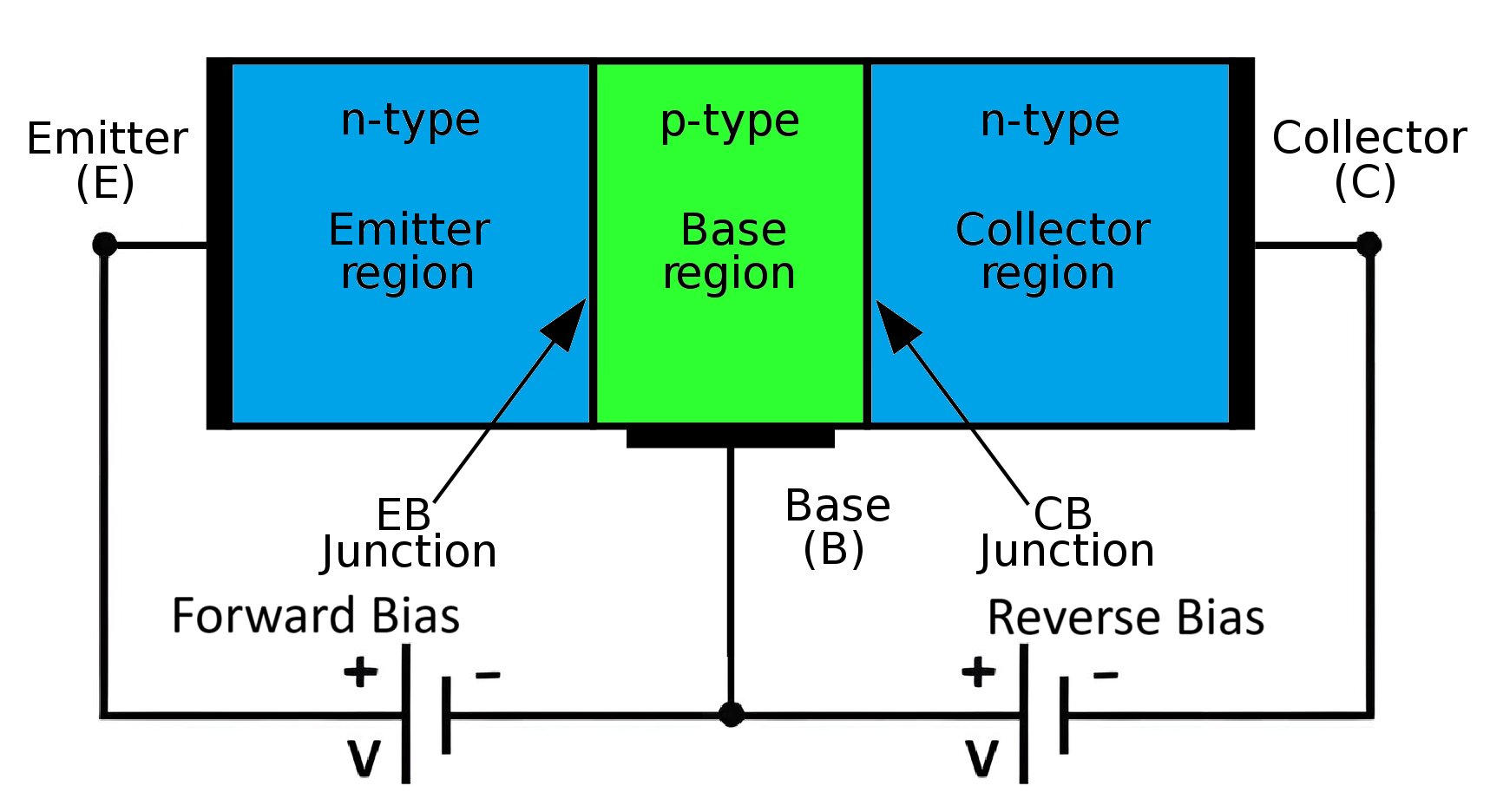
When a small positive voltage is applied across the base-emitter junction, the emitter-base junction becomes forward biased. Electrons are injected from the emitter into the base. Since the base is extremely thin and lightly doped, most of these electrons pass through the base without recombining and are attracted toward the collector by the reverse-biased collector-base junction.
This movement of electrons produces the collector current. As a result, a very small base current controls a much larger collector current.
- Majority charge carriers are electrons.
- Electrons flow from the emitter toward the collector.
- Conventional current flows from the collector to the emitter.
- A positive base current turns the transistor ON.
- Widely used because electrons have higher mobility, resulting in faster switching speed.
PNP Transistor
In a PNP transistor, the emitter is heavily doped P-type material, the base is thin and lightly doped N-type material, and the collector is moderately doped P-type material.
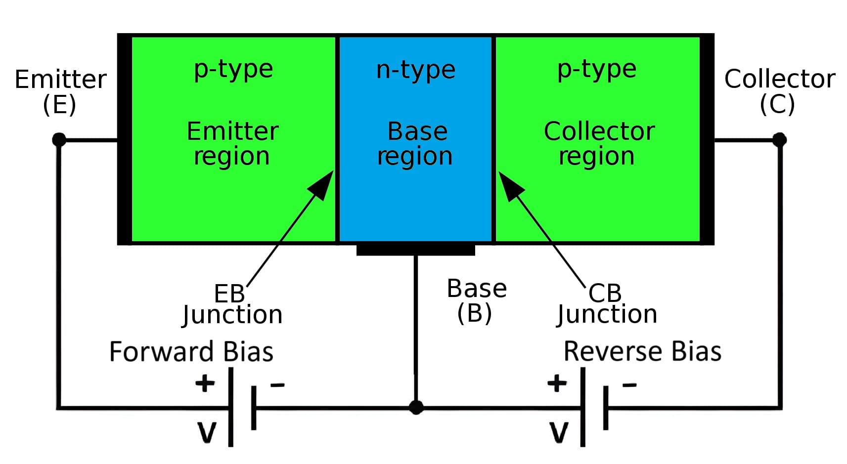
When a small negative voltage is applied to the base with respect to the emitter, the emitter-base junction becomes forward biased. Holes are injected from the emitter into the base. Due to the thin base region, most holes pass through the base and are collected by the collector through the reverse-biased collector-base junction.
This movement of holes creates the collector current. Similar to the NPN transistor, only a small base current is required to control a much larger collector current.
- Majority charge carriers are holes.
- Holes move from the emitter toward the collector.
- Conventional current flows from the emitter to the collector.
- A negative base voltage relative to the emitter turns the transistor ON.
- Commonly used in complementary transistor circuits and high-side switching applications.
Biasing of Bipolar Junction Transistor (BJT)
For a Bipolar Junction Transistor to operate correctly, appropriate voltages must be applied across its two PN junctions. This process is known as biasing. The biasing condition determines whether the transistor acts as an amplifier, an electronic switch, or remains in the OFF state.
A BJT contains two PN junctions:
- Emitter-Base Junction (EB Junction)
- Collector-Base Junction (CB Junction)
Depending on whether these junctions are forward biased or reverse biased, the transistor operates in different regions.
Operating Regions of a BJT
A Bipolar Junction Transistor can operate in four different regions depending on the biasing applied to its emitter-base and collector-base junctions.
| Operating Region | Emitter-Base Junction | Collector-Base Junction | Typical Application |
|---|---|---|---|
| Cut-off Region | Reverse Biased | Reverse Biased | Transistor OFF (Open Switch) |
| Active Region | Forward Biased | Reverse Biased | Signal Amplification |
| Saturation Region | Forward Biased | Forward Biased | Transistor ON (Closed Switch) |
| Reverse Active Region | Reverse Biased | Forward Biased | Rarely Used |
Active Region
The active region is the normal operating region when a BJT is used as an amplifier.
- The emitter-base junction is forward biased.
- The collector-base junction is reverse biased.
- A small base current controls a much larger collector current.
- The collector current is approximately proportional to the base current.
Most analog amplifier circuits operate in the active region because the transistor provides excellent current and voltage gain.
Cut-off Region
In the cut-off region, both the emitter-base junction and collector-base junction are reverse biased.
- Both PN junctions are reverse biased.
- Base current is nearly zero.
- Collector current is almost zero.
- The transistor behaves like an open switch.
This operating region is commonly used when the transistor functions as an electronic switch in the OFF state.
Saturation Region
In the saturation region, both PN junctions are forward biased.
- The emitter-base junction is forward biased.
- The collector-base junction is also forward biased.
- The collector current reaches its maximum value.
- Further increases in base current produce little change in collector current.
When operating in saturation, the transistor behaves like a closed switch and is widely used in switching circuits such as relay drivers, LED drivers, and motor control circuits.
Reverse Active Region
In the reverse active region, the emitter-base junction is reverse biased while the collector-base junction is forward biased.
- Emitter-base junction is reverse biased.
- Collector-base junction is forward biased.
- The collector and emitter exchange their normal roles.
- Current gain is very low.
This operating mode is rarely used in practical electronic circuits because the transistor provides poor amplification under these conditions.
VI Characteristics of Bipolar Junction Transistors (BJTs)
The Voltage-Current (VI) characteristics of a Bipolar Junction Transistor (BJT) describe the relationship between the voltages and currents at its three terminals: the emitter, base, and collector. These characteristics are essential for understanding transistor operation and are widely used in the analysis and design of amplifier and switching circuits.
Since BJTs are available in both NPN and PNP configurations, the VI characteristics are similar in shape but differ in the polarity of the applied voltages and current directions.
VI Characteristics of NPN Transistor
The VI characteristics of an NPN transistor are generally studied using the Common Emitter (CE) configuration because it provides high current and voltage gain, making it the most widely used transistor configuration.
Input Characteristics (Base-Emitter Junction)
The input characteristics show the relationship between the base current (IB) and the base-emitter voltage (VBE).

- Configuration: Common Emitter (CE)
- Plot: Base Current (IB) versus Base-Emitter Voltage (VBE).
- Behavior: Similar to a forward-biased PN junction diode. As the base-emitter voltage increases, the base current increases exponentially.
For a silicon transistor, the base-emitter junction typically begins conducting at approximately 0.7 V.
Output Characteristics (Collector-Emitter Junction)
The output characteristics represent the relationship between the collector current (IC) and the collector-emitter voltage (VCE) for different values of base current.
- Configuration: Common Emitter (CE)
- Plot: Collector Current (IC) versus Collector-Emitter Voltage (VCE) for various values of Base Current (IB).
The output characteristics are divided into three important operating regions.
- Cut-off Region: Both the emitter-base and collector-base junctions are reverse biased. The collector current is almost zero, and the transistor behaves like an open switch.
- Active Region: The emitter-base junction is forward biased while the collector-base junction is reverse biased. The collector current is primarily determined by the base current (IC ≈ β × IB), making this region suitable for amplification.
- Saturation Region: Both PN junctions are forward biased. The collector current reaches its maximum value, and further increases in collector-emitter voltage produce very little change in collector current.


- For a fixed value of base current, the collector current initially increases with collector-emitter voltage and then becomes nearly constant in the active region.
- Once the transistor enters the saturation region, increasing the collector-emitter voltage has very little effect on the collector current.
VI Characteristics of PNP Transistor
The VI characteristics of a PNP transistor are almost identical to those of an NPN transistor. The primary difference is that the polarity of the applied voltages and current directions is reversed.
Input Characteristics (Base-Emitter Junction)
- Configuration: Common Emitter (CE)
- Plot: Base Current (IB) versus Base-Emitter Voltage (VBE).
- Behavior: Similar to a forward-biased diode but with reverse polarity compared to an NPN transistor. As the magnitude of the negative base-emitter voltage increases, the base current increases exponentially.
Output Characteristics (Collector-Emitter Junction)
- Configuration: Common Emitter (CE)
- Plot: Collector Current (IC) versus Collector-Emitter Voltage (VCE) for different values of Base Current (IB).
The output characteristics also consist of the same three operating regions.
- Cut-off Region: Both the emitter-base and collector-base junctions are reverse biased. The collector current is almost zero.
- Active Region: The emitter-base junction is forward biased while the collector-base junction is reverse biased. The collector current is primarily controlled by the base current (IC ≈ β × IB).
- Saturation Region: Both PN junctions are forward biased, and the collector current reaches its maximum value with little change despite increases in collector-emitter voltage.
- For a given base current, the collector current initially increases as the collector-emitter voltage increases in the negative direction and then becomes nearly constant in the active region.
- Once the transistor enters saturation, further increases in collector-emitter voltage produce only a very small change in collector current.
Important Points
- Common Emitter (CE) is the most widely used transistor configuration because it provides excellent current and voltage gain.
- The collector current (IC) depends primarily on the base current (IB) while the transistor operates in the active region.
- The base-emitter junction of a silicon BJT typically requires approximately 0.7 V to conduct.
- The Active Region is used for amplification applications.
- The Saturation Region is used when the transistor functions as a closed electronic switch.
- The Cut-off Region represents the OFF state of the transistor and is widely used in switching circuits.
- The VI characteristics provide valuable information for selecting the appropriate operating region while designing amplifier and switching circuits.
Understanding the VI characteristics of a Bipolar Junction Transistor is essential for analyzing electronic circuits, designing amplifiers, and developing reliable switching applications.
Advantages and Disadvantages of BJT
Like every semiconductor device, a Bipolar Junction Transistor (BJT) has its own advantages and limitations. Its excellent current amplification, linearity, and low manufacturing cost make it suitable for numerous analog and digital applications. However, BJTs also have certain drawbacks, such as lower input impedance and higher power consumption compared to Field Effect Transistors (FETs).
Advantages of BJT
- High Current Gain: BJTs provide excellent current gain, making them ideal for amplification applications.
- Good Voltage Gain: They can produce significant voltage amplification in amplifier circuits.
- Excellent Frequency Response: BJTs perform well in high-frequency applications such as RF amplifiers.
- Low Saturation Voltage: They exhibit a low collector-emitter saturation voltage, reducing power loss when used as switches.
- Good Linearity: BJTs provide better linear amplification, making them highly suitable for analog electronic circuits.
- Ease of Biasing: Proper biasing techniques allow stable transistor operation across different applications.
- Reliable Performance: BJTs offer reliable operation over a wide range of operating conditions.
- Low Manufacturing Cost: They are inexpensive and widely available in numerous voltage and current ratings.
- Suitable for Analog and Digital Circuits: BJTs are extensively used in amplifiers, oscillators, switching circuits, and signal conditioning applications.
Disadvantages of BJT
- Higher Power Consumption: BJTs generally consume more power than Field Effect Transistors (FETs), particularly in high-frequency circuits.
- Heat Generation: Higher power dissipation results in increased heat generation, often requiring heat sinks in power applications.
- Lower Input Impedance: Compared to FETs, BJTs have lower input impedance, which may load the previous stage.
- Requires Continuous Base Current: Since BJTs are current-controlled devices, a continuous base current is required during operation.
- Switching Speed: BJTs are generally slower than modern MOSFETs in high-speed switching applications.
- Thermal Runaway: Improper biasing may lead to thermal runaway, affecting device reliability.
- More Complex Biasing for Precision Circuits: Some applications require carefully designed biasing networks to maintain stable operation.
Applications of Bipolar Junction Transistors
Because of their excellent amplification and switching capabilities, Bipolar Junction Transistors are widely used in almost every branch of electronics. Their ability to control a large collector current using a relatively small base current makes them suitable for both low-power and high-power electronic systems.
Amplification Applications:
- Audio Amplifiers: Amplify weak audio signals for speakers and sound systems.
- Voltage Amplifiers: Increase the voltage level of low-amplitude signals.
- Current Amplifiers: Provide higher output current for various electronic circuits.
- Radio Frequency (RF) Amplifiers: Amplify high-frequency signals used in communication systems.
Switching Applications:
- Digital Switching Circuits
- Relay Driver Circuits
- LED Driver Circuits
- Motor Driver Circuits
- Power Switching Circuits
Signal Generation Applications:
Power Electronics Applications:
- Voltage Regulators
- Current Sources
- Power Supply Control Circuits
- Battery Charging Circuits
Communication Systems:
- Signal Modulation Circuits
- RF Communication Equipment
- Wireless Communication Systems
- Instrumentation Circuits
Industrial Applications:
- Industrial Automation Systems
- Motor Speed Controllers
- Sensor Interface Circuits
- Control Systems
Other Common Applications:
- Darlington Pair Circuits
- Current Mirror Circuits
- Operational Amplifier Internal Stages
- Analog-to-Digital Converters (ADC)
- Digital-to-Analog Converters (DAC)
- Temperature Sensing Circuits
- Electronic Timers
Even though MOSFETs have replaced BJTs in many high-speed switching applications, BJTs remain indispensable in analog electronics because of their excellent linearity, predictable gain characteristics, and low manufacturing cost.
BJT Summary
A Bipolar Junction Transistor (BJT) is a three-terminal semiconductor device that controls the flow of current using a relatively small base current. Since both electrons and holes participate in current conduction, it is known as a bipolar device. BJTs are available in two types NPN and PNP and consist of three semiconductor regions known as the emitter, base, and collector.
The emitter-base junction and collector-base junction work together to control the movement of charge carriers. Depending on the applied bias, a transistor operates in the cut-off, active, saturation, or reverse-active region, allowing it to function as either an amplifier or an electronic switch.
Due to their excellent current gain, good linearity, low cost, and reliable performance, Bipolar Junction Transistors continue to play an important role in analog electronics, communication systems, industrial automation, instrumentation, and power control circuits.
Frequently Asked Questions (FAQs)
What is a Bipolar Junction Transistor (BJT)?
A Bipolar Junction Transistor (BJT) is a three-terminal semiconductor device used to amplify or switch electronic signals. It controls a large collector current using a much smaller base current.
Why is it called a Bipolar Junction Transistor?
The term bipolar refers to the participation of both electrons and holes in current conduction, while junction refers to the two PN junctions formed inside the transistor.
What are the two types of BJTs?
The two types of Bipolar Junction Transistors are:
- NPN Transistor
- PNP Transistor
What are the three terminals of a BJT?
The three terminals of a Bipolar Junction Transistor are:
- Emitter (E)
- Base (B)
- Collector (C)
Why is the base region very thin?
The base is made extremely thin and lightly doped so that most charge carriers injected by the emitter can pass through to the collector with minimal recombination, resulting in high current gain.
Why is the collector larger than the emitter?
The collector is physically larger because it must withstand higher voltages and dissipate more heat during transistor operation.
Is a BJT a current-controlled or voltage-controlled device?
A Bipolar Junction Transistor is a current-controlled semiconductor device because the collector current is controlled by the base current.
What is the difference between an NPN and a PNP transistor?
An NPN transistor uses electrons as the majority charge carriers, whereas a PNP transistor uses holes. They also differ in current direction and biasing polarity.
Where are BJTs commonly used?
BJTs are widely used in:
- Audio amplifiers
- RF amplifiers
- Switching circuits
- Oscillators
- Power supplies
- Communication equipment
- Industrial automation systems
- Voltage regulators
- Motor control circuits
IGBT Full Form, Symbol, Construction, Working and Applications
JFET Junction Field Effect Transistors Working and Applications
UJT Unijunction Transistor Symbol, Construction, Working & Applications
Difference Between Photodiode, Phototransistor and Photoresistor
Types of Transistors: Classification (BJT, JFET, MOSFET & IGBT)
Unbiased PN Junction: Depletion Region and Barrier Potential

