Drift current and diffusion current are two fundamental mechanisms of charge transport in semiconductors. These concepts form the basis of semiconductor physics and are extremely important for understanding the operation of devices such as p-n junction diodes, transistors, LEDs, solar cells, MOSFETs, and integrated circuits.
In semiconductors, electric current is produced not only by the movement of charge carriers under an applied electric field but also by the movement of carriers caused by concentration differences. The current caused by an electric field is known as drift current, while the current caused by charge concentration gradient is called diffusion current.
Understanding these two types of currents is essential for studying modern electronics and semiconductor device theory.
Related Articles:
- Intrinsic Semiconductors Explained
- Extrinsic Semiconductors Explained
- Difference Between Intrinsic and Extrinsic Semiconductor
- LED – Symbol, Construction, Working, Types and Applications
- Energy Band Theory of Solids: Conductors, Semiconductors, and Insulators
Current in a Semiconductor
Electric current in a semiconductor is produced by the movement of charge carriers. These charge carriers are:
- Free electrons in the conduction band
- Holes in the valence band
Unlike conductors where only electrons participate in conduction, semiconductors allow conduction through both electrons and holes.
The total current in a semiconductor is generally the combination of:
I = Idrift + Idiffusion
- Idrift = Drift current
- Idiffusion = Diffusion current
Drift Current in Semiconductors
Definition of Drift Current
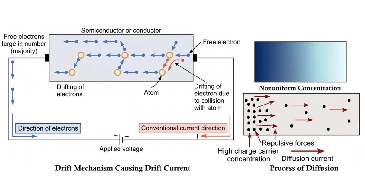
The electric current produced in a semiconductor due to the movement of charge carriers under the influence of an externally applied electric field is called drift current.
When a voltage is applied across a semiconductor material, free electrons and holes experience an electric force. Because of this force, electrons drift toward the positive terminal while holes drift toward the negative terminal, producing electric current.

Working Principle of Drift Current
When no external voltage is applied, the free electrons move randomly inside the semiconductor due to thermal energy. Since the movement is random, the net current becomes zero.
When an external electric field is applied:
- Electrons move opposite to the electric field direction
- Holes move in the direction of the electric field
- The random motion still exists and electrons collide with atoms
- However, an average directional motion is established
This average motion of charge carriers is called drift.
Drift of Electrons
Electrons are negatively charged particles. Therefore:
- They are repelled by the negative terminal
- They are attracted toward the positive terminal
During movement, electrons continuously collide with semiconductor atoms, crystal lattice and impurity atoms. Because of these collisions, electrons do not move in a perfectly straight line. Instead, they follow a zigzag path while slowly drifting toward the positive terminal.
Drift of Holes
Holes behave as positive charge carriers. Therefore:
- They are repelled by the positive terminal
- They are attracted toward the negative terminal
When an electric field is applied, holes appear to move through the semiconductor toward the negative terminal. In reality, electrons from neighboring covalent bonds continuously jump to fill nearby holes, creating new holes behind them. Due to repeated collisions with semiconductor atoms, crystal lattice vibrations, and impurity atoms, hole movement is not perfectly straight. Instead, holes also follow a zigzag path while slowly drifting toward the negative terminal.
Drift Velocity
The average velocity acquired by charge carriers under the applied electric field is called drift velocity.
vd = μE
- vd = Drift velocity
- μ = Mobility of charge carriers
- E = Applied electric field intensity
The drift velocity is directly proportional to the electric field.
Formula for Drift Current
The drift current density for electrons is:
Jn = qnμnE
The drift current density for holes is:
Jp = qpμpE
The total drift current density becomes:
Jdrift = q(nμn + pμp)E
- J = Current density
- q = Electronic charge ((1.6 × 10⁻¹⁹ C))
- n = Electron concentration
- p = Hole concentration
- μn = Electron mobility
- μp = Hole mobility
- E = Electric field intensity
Important Points About Drift Current
- Drift current requires an external electric field.
- Both electrons and holes contribute to drift current.
- Drift current exists in conductors and semiconductors.
- The direction of electron flow is opposite to conventional current.
- Drift current increases with electric field intensity.
Conventional Current Direction
The conventional current direction is always considered from positive terminal to negative terminal. Electrons actually move from negative to positive terminal and semiconductor device operation is often explained using electron flow.
Electron Flow Direction ≠ Conventional Current Direction
Mobility of Charge Carriers
Mobility indicates how easily charge carriers move through a semiconductor under an electric field.
μ = vd/E
Higher mobility means faster carrier movement, greater conductivity and higher drift current. Electron mobility is generally higher than hole mobility.
Diffusion Current in Semiconductors
Definition of Diffusion Current
The electric current produced due to the movement of charge carriers from a region of higher concentration to a region of lower concentration is called diffusion current.
Diffusion current occurs because semiconductors may have nonuniform carrier concentration. Unlike drift current, diffusion current does not require an externally applied voltage.

Cause of Diffusion Current
Diffusion occurs when one region contains a large number of carriers and another region contains fewer carriers; this creates a concentration gradient. Charge carriers naturally move from higher concentration to lower concentration to achieve uniform distribution.
Diffusion Process in P-Type Semiconductor
Consider a nonuniformly doped p-type semiconductor:
- One side has high hole concentration
- The other side has low hole concentration
Because holes are densely packed on one side:
- Repulsive forces exist between holes
- Holes start moving toward the low concentration region
This movement of holes creates diffusion current.
Diffusion Process in N-Type Semiconductor
In a nonuniformly doped n-type semiconductor:
- One side has more free electrons
- The other side has fewer free electrons
Electrons diffuse from higher concentration to lower concentration, thus producing diffusion current.

Diffusion Current Density Formula
The diffusion current density for electrons is:
Jn = qDndn/dx
The diffusion current density for holes is:
Jp = -qDpdp/dx
The total diffusion current density becomes:
Jdiffusion = qDndn/dx - qDpdp/dx
- Dn = Electron diffusion coefficient
- Dp = Hole diffusion coefficient
- dn/dx = Electron concentration gradient
- dp/dx = Hole concentration gradient
Characteristics of Diffusion Current
- Diffusion current occurs due to concentration gradient.
- No external electric field is required.
- It is unique to semiconductors.
- It mainly occurs in nonuniformly doped semiconductors.
- Diffusion plays a major role in p-n junction operation.
Einstein’s Relation
The diffusion coefficient and mobility are related by Einstein’s equation:
D/μ = kT/q
- D = Diffusion coefficient
- μ = Mobility
- k = Boltzmann constant
- T = Absolute temperature
- q = Electronic charge
At room temperature: kT/q ≈ 0.026V
Difference Between Drift Current and Diffusion Current
| Parameter | Drift Current | Diffusion Current |
|---|---|---|
| Cause | Applied electric field | Carrier concentration gradient |
| External Voltage | Required | Not necessary |
| Direction of Carrier Movement | Due to electric force | From high to low concentration |
| Occurs In | Conductors and semiconductors | Mainly semiconductors |
| Dependency | Electric field intensity | Concentration gradient |
| Carrier Motion | Drift motion | Diffusion motion |
| Importance | Current conduction | PN junction formation |
Drift and Diffusion in PN Junction Diode
The operation of a PN junction diode is based on both drift and diffusion currents.
Diffusion Current in PN Junction: Majority carriers move across the junction due to concentration gradient. Electrons diffuse from n-side to p-side. Holes diffuse from p-side to n-side.
Drift Current in PN Junction: After diffusion a depletion region is formed, and an internal electric field develops. Minority carriers move due to this electric field which creates drift current.

At equilibrium:
Idrift = Idiffusion
Hence, net current becomes zero.
In practical semiconductor devices, both drift and diffusion currents exist simultaneously.
Total Semiconductor Current Density Equation:
Jtotal = Jdrift + Jdiffusion
Advantages, Disadvantages and Applications
Advantages of Drift Current
- Fast carrier movement due to applied electric field.
- Easy to control by changing voltage or electric field.
- Suitable for high-speed electronic devices.
- Provides stable current flow in circuits.
- Essential for amplification and switching in transistors.
- Efficient for long-distance carrier transport in semiconductors.
Disadvantages of Drift Current
- Requires external electric field or voltage supply.
- Causes power consumption and heating.
- High electric fields may damage semiconductor devices.
- Carrier mobility decreases at high temperatures.
- Can lead to breakdown effects in semiconductors.
Advantages of Diffusion Current
- Does not require external voltage for carrier movement.
- Naturally occurs due to concentration difference.
- Important for PN junction formation and device operation.
- Useful in semiconductor fabrication processes.
- Helps in minority carrier transport in devices like solar cells and LEDs.
Disadvantages of Diffusion Current
- Generally slower than drift current.
- Difficult to control precisely.
- Strongly affected by temperature changes.
- Limited by carrier recombination losses.
- Cannot alone provide efficient current transport in many practical circuits.
Applications of Drift Current
- Operation of PN junction diodes under bias.
- Current flow in transistors such as BJT transistor and MOSFET.
- Working principle of semiconductor resistors.
- Charge transport in integrated circuits (ICs).
- Functioning of photodiodes and solar cells under electric fields.
- Carrier movement in semiconductor detectors.
- Used in high-speed electronic switching devices.
- Essential for operation of electric-field-controlled devices like FETs.
- Basis of conduction in conductors and semiconductors when voltage is applied.
- Important in power electronics and rectifier circuits.
Applications of Diffusion Current
- Formation and operation of PN junctions.
- Carrier transport in unbiased semiconductors.
- Working of LEDs and semiconductor lasers.
- Important in transistor action inside BJTs.
- Used in solar cells for minority carrier transport.
- Essential in charge recombination and injection processes.
- Helps in understanding semiconductor doping profiles.
- Important in microelectronics fabrication during impurity diffusion.
- Used in sensor devices and diffusion-based semiconductor devices.
- Plays a major role in carrier distribution analysis in semiconductor physics.
Conclusion
Drift current and diffusion current are the two primary charge transport mechanisms in semiconductors. Drift current occurs because of the movement of charge carriers under an externally applied electric field, while diffusion current occurs because of carrier concentration differences inside the semiconductor material.
Both mechanisms are equally important in understanding semiconductor device operation. Drift current dominates when an electric field is applied, whereas diffusion current becomes significant in nonuniformly doped regions and p-n junctions. Modern semiconductor devices such as diodes, transistors, LEDs, and integrated circuits rely heavily on the combined effects of these two currents for proper operation.
A clear understanding of drift current and diffusion current forms the foundation for advanced semiconductor electronics and device engineering.
Energy Band Theory of Solids: Conductors, Semiconductors, and Insulators
Types of Diodes: Symbol, Working, Characteristics and Applications
