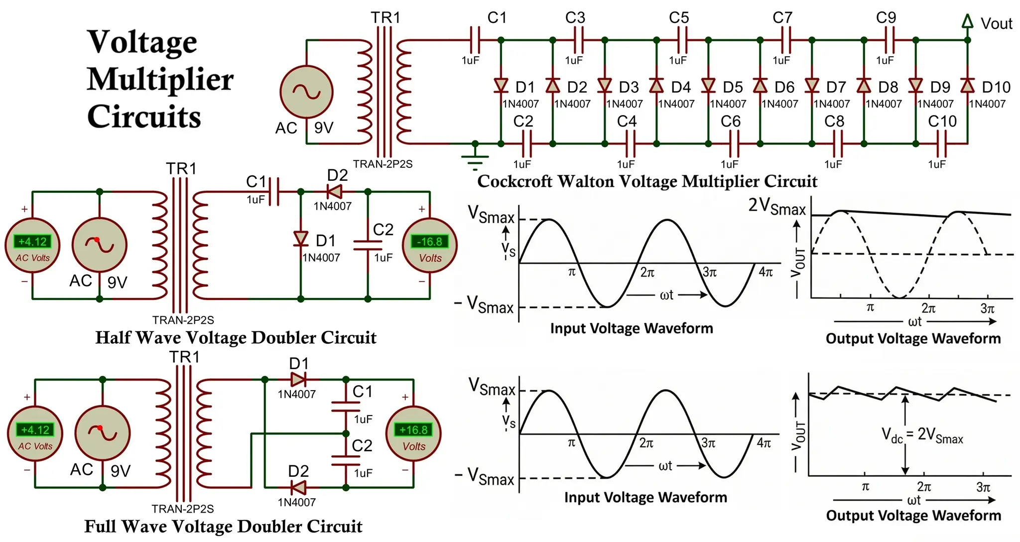
Voltage Multiplier Circuit Diagram, Working, Types and Applications
Voltage multiplier circuit forms a fundamental building block in high-voltage power supplies where the output voltage must be several times greater than the peak input… Read More »Voltage Multiplier Circuit Diagram, Working, Types and Applications