A NOR Gate (NOT-OR Gate) is one of the most fundamental logic gates in digital electronics. It performs a Boolean operation that is the complement of the OR operation, meaning its output is the inverse of an OR gate.
In simple terms, a NOR gate produces an output HIGH (1) only when all inputs are LOW (0). If any one of the inputs is HIGH, the output becomes LOW.
NOR gates are extremely important because they are classified as universal gates, which means any digital logic circuit can be implemented using only NOR gates. This makes them highly valuable in digital design and integrated circuit fabrication.
They are widely used in applications such as logic circuit design, memory elements (like SR latches), control circuits, and digital systems where inversion combined with OR functionality is required.
One of the key reasons for their importance is that NOR logic can replicate all other basic gates (AND, OR, NOT), making it a foundational building block in digital electronics.
- Related Articles:
- Types of Logic Gates with Symbol, Truth Table and IC Numbers
- NAND Gate Truth Table, Logic Circuit & IC 7400 Pin Diagram
- OR Gate: Symbol, Truth Table, Logic Circuit, and IC Numbers
- AND Gate: Symbol, Truth Table, Logic Circuit, and IC Numbers
- Buffer Gate: Symbol, Truth Table, Circuit, Types and IC Numbers
- NOT Gate: Symbol, Truth Table, Logic Circuit, and IC Numbers
- XOR Gate: Symbol, Truth Table, Logic Circuit, and IC Numbers
- XNOR Gate: Symbol, Truth Table, Logic Circuit, and IC Numbers
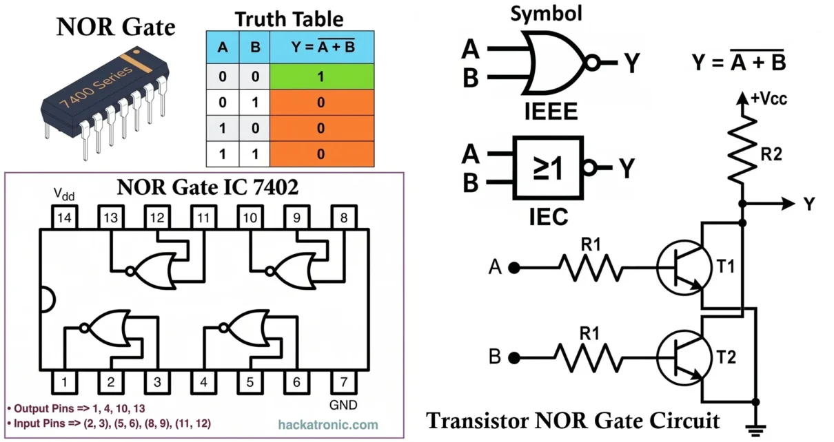
Symbol of NOR Gate
- Standard Symbol (ANSI)
- The most commonly used NOR gate symbol (ANSI standard) consists of:
- A shape similar to the OR gate
- A small bubble (inversion circle) at the output
- Two or more input lines entering from the left
- One output line exiting from the right
- This output bubble represents the inversion of OR logic, which converts an OR gate into a NOR gate.
- The most commonly used NOR gate symbol (ANSI standard) consists of:

- IEC Symbol
- Represented as a rectangle
- Inside marking: ≥1 with an inversion indication (bubble or bar)
- Inputs enter from the left, output exits from the right
- Multi-Input Symbol
- Additional input lines can be added on the left
- Logic: Output is HIGH only when all inputs are LOW
- Terminal and Notation
- Inputs: A, B, C, D…
- Output: Y or Q
- Boolean expression: Y = (A + B)’
- For multiple inputs: Y = (A + B + C + …)’
- Important Observations
- Output is HIGH only when all inputs are LOW
- NOR is the complement of OR gate
- Acts as a universal logic gate
- Removing the output bubble → becomes OR gate
- Can be used to implement any other logic gate
- Widely used in latches, memory circuits, and control logic
Truth Table of NOR Gate
- Working Principle
- The NOR gate operates based on the inversion of the OR operation:
- Output is HIGH (1) only when all inputs are LOW (0)
- Output is LOW (0) if any input is HIGH (1)
- Unlike the OR gate, which gives HIGH output when at least one input is HIGH, the NOR gate produces the exact opposite result due to the inversion at the output.
- The NOR gate operates based on the inversion of the OR operation:
- Boolean Logic
- The NOR operation follows the Boolean expression: Y = (A + B)’
- For multiple inputs: Y = (A + B + C + …)’
- This is why it is called a NOT-OR gate, as it is simply the complement of the OR operation.

- Key Condition
- All inputs LOW → Output = HIGH
- Any input HIGH → Output = LOW
- If A = 0 and B = 0 → Y = 1
- If A = 0 and B = 1 → Y = 0
- If A = 1 and B = 0 → Y = 0
- If A = 1 and B = 1 → Y = 0
- This makes the NOR gate behave as a zero detector, since it only produces HIGH when all inputs are zero.

- Key Observation
- Output is HIGH only when all inputs are LOW
- Output is LOW if any one or more inputs are HIGH
- Extended Form: Y = (A + B + C + D …)’
- Truth Table Insight
- NOR gate acts as a universal logic element
- Can be used to implement NOT, OR, AND, and any complex logic function
- Forms the basis of memory elements like SR latch
- Important in control logic and digital system design
- Multi-Input NOR Gates
- Can have more than 2 inputs
- Output depends on the condition that all inputs must be LOW
NOR gates are widely used in digital logic design, memory circuits (latches and flip-flops), control and automation systems, Arithmetic and Logic Units (ALUs), signal inversion and decision-making circuits
NOR Logic Circuits
Implementation of NOR gate is simple because it is directly derived from OR logic followed by inversion.
- NOR is widely implemented using:
- Basic gates (OR + NOT)
- Transistor logic (RTL / TTL)
- CMOS structures
Since NOR is itself a universal gate, any digital logic function can be constructed using only NOR gates, making it extremely important in practical circuit design.
Diode NOR Gate (Diode-Transistor Logic)
- Components: Diodes, Transistor and Resistors
- Working
- A pure diode based NOR gate is not very practical
- When any input is HIGH, the corresponding diode becomes forward biased
- This creates a conduction path, pulling the output toward LOW after inversion
- However, due to the presence of proper inversion and amplification stage (transistor), diode-transistor logic produces a strong NOR output
- Working

- Key Behavior
- Diodes provide OR-like conduction
- Additional inversion is required to obtain NOR logic
- Limitation
- Cannot provide proper logic levels alone
- Voltage drop across diodes affects output
- Poor noise margin
- Not used in modern digital circuits
Transistor NOR Gate (RTL / TTL)
- Components
- Transistors (T1, T2)
- Resistor (pull-up resistor)
- Working Principle
- Transistors act as switches connected in parallel configuration
- Output is taken from the collector node

- Operation
- When any input is HIGH: Corresponding transistor turns ON → output is pulled to ground → Output = LOW
- When all inputs are LOW: All transistors remain OFF → no conduction path to ground → pull-up resistor drives output HIGH
- Key Insight
- Parallel transistor network performs OR operation
- Output inversion naturally produces NOR logic
- Simple and efficient implementation
CMOS NOR Gate
- Structure
- Built using complementary MOSFETs:
- PMOS (pull-up network)
- NMOS (pull-down network)
- Built using complementary MOSFETs:
- Configuration
- PMOS transistors connected in series
- NMOS transistors connected in parallel

- Working
- When all inputs are LOW: PMOS network conducts → output pulled HIGH
- When any input is HIGH: Corresponding NMOS conducts → output pulled LOW
- Advantages
- Very low power consumption
- High noise immunity
- Excellent switching performance
- Widely used in VLSI and IC design
This is the most practical and widely used NOR implementation in modern electronics.
NOR Using OR and NOT Gates
- Boolean Expression: Y = (A + B)̅
- Implementation
- One OR gate
- One NOT gate (inverter)

- Working
- OR gate produces A + B
- Inverter flips the result
- Final output becomes NOR
- Key Insight
- NOR is simply OR followed by NOT
- Most fundamental and easiest way to understand NOR logic
NOR Using NAND Gates
- Boolean Expression: Y = (A + B)̅
- Using De Morgan’s Theorem: Y = (A̅ · B̅)
- Implementation
- Four NAND gates
- Two NAND gates used as inverters
- One NAND gate for intermediate operation
- Final NAND used for inversion

- Working
- First NAND gate inverts A → A̅
- Second NAND gate inverts B → B̅
- Third NAND gate performs: (A̅ · B̅)̅ = A + B
- Final NAND (self-connected) inverts output → (A + B)̅
- Simplified NAND-Only Structure
- A NAND A → A̅
- B NAND B → B̅
- (A̅ NAND B̅) → A + B
- Output NAND itself → NOR output
- Key Insight
- NOR can be built using only NAND gates
- Based on De Morgan’s theorem
- Useful when only NAND gates are available in hardware
Implementing All Logic Gates Using NOR Gate
Due to its universal nature, a NOR gate can be used to construct all other basic logic gates. This is one of the most important theoretical and practical properties of the NOR gate in digital electronics.
NOT Gate Using a NOR Gate
A NOT gate (inverter) can be implemented by connecting both inputs of a NOR gate to the same signal:

- Boolean Expression: Y = (A + A)̅ = A̅
- Working:
- When A = 0 → Y = 1
- When A = 1 → Y = 0
- Key Insight:
- A NOR gate can directly act as an inverter
- This is the simplest possible implementation using NOR
OR Gate Using NOR Gates
An OR gate can be realized by double inversion using NOR gates:

- Boolean Expression: OR = A + B = ( (A + B)̅ )̅
- Implementation:
- First NOR gate: produces (A + B)̅
- Second NOR gate (as inverter): inverts output
- Working:
- First stage gives NOR output
- Second stage restores original OR function
- Key Insight:
- OR = NOR followed by NOT
- Requires two NOR gates
AND Gate Using NOR Gates
Using De Morgan’s Theorem, an AND gate can be constructed from NOR gates:

- Boolean Expression: AND = A · B = (A̅ + B̅)̅
- Implementation:
- First, invert inputs using NOR-based NOT gates:
- A̅ = A NOR A
- B̅ = B NOR B
- Then apply NOR to these inverted inputs
- Working:
- Input inversion stage
- Followed by NOR operation
- Produces AND output
- Key Insight:
- AND is obtained by NOR of inverted inputs
- Requires three NOR gates
NAND Gate Using NOR Gates
A NAND gate can be constructed by combining AND and NOT operations:

- Boolean Expression: NAND = (A · B)’
- Implementation:
- First construct AND using NOR gates
- Then invert the result using a NOR-based NOT gate
- Working:
- AND stage produces A·B
- Final inversion gives NAND output
- Key Insight:
- NAND = AND followed by NOT
- Requires multiple NOR stages
XOR Gate Using NOR Gates
An XOR gate can be implemented using multiple NOR gates, though it becomes more complex:

- Boolean Expression: XOR = A ⊕ B = A̅B + AB̅
- Conceptual Implementation:
- Generate inverted inputs
- Create conditional paths for unequal inputs
- Combine using NOR logic
- Working Insight:
- Output is HIGH when inputs are different
- Achieved through multiple intermediate NOR stages
- Key Insight:
- XOR is more complex using NOR compared to NAND
- Requires careful arrangement of logic
XNOR Gate Using NOR Gates
- An XNOR gate can be constructed by either:
- Inverting XOR output, or
- Direct NOR-based implementation

- Boolean Expression: XNOR = (A ⊕ B)’ = A ⊙ B = AB + A̅B̅
- NOR Implementation: Y = (A NOR (A NOR B)) NOR (B NOR (A NOR B))
- Working:
- Intermediate NOR operations generate required complements
- Final NOR stage combines them to detect equality
- Key Insight:
- NOR implementation of XNOR is often more natural than NAND
- Efficient in CMOS where NOR structures are preferred
- NOR gate alone can implement all fundamental logic gates
- This eliminates the need for multiple gate types
- Highly beneficial in IC fabrication and VLSI design
- Demonstrates the functional completeness of NOR logic
NOR Gate IC Numbers and Details
NOR gates are widely available in both TTL (Transistor-Transistor Logic) and CMOS logic families. Since NOR is a basic universal gate, these ICs are very common and extensively used in digital circuit design.
NOR Gate IC 7402 (TTL Quad NOR Gate)
The 7402 NOR Gate IC is one of the most commonly used NOR gate ICs from the TTL family.

- Features
- Quad 2-input NOR gates (4 NOR gates in one IC)
- Technology: TTL (BJT-based)
- Fast switching speed
- Standard push-pull output
- Propagation delay: ~10 ns
- Supply voltage: 5V (fixed)
- Pin Configuration
- Total pins: 14
- Gate Configuration:
- Gate 1: Pins 1, 2 → Output 3
- Gate 2: Pins 4, 5 → Output 6
- Gate 3: Pins 9, 10 → Output 8
- Gate 4: Pins 12, 13 → Output 11
- Power Pins:
- Pin 14: Vcc (+5V)
- Pin 7: GND
- Key Characteristic
- Each gate operates independently
- Widely used in TTL-based digital systems
- Suitable for moderate-speed applications
74HC02 – CMOS NOR Gate
The 74HC02 NOR Gate IC belongs to the High-Speed CMOS family.
- Specifications
- Technology: CMOS
- Supply voltage: 2V to 6V
- Power consumption: Very low
- Propagation delay: ~8–15 ns
- Output type: Push-pull
- Key Characteristic
- Combines high speed with low power consumption
- Suitable for modern digital circuits and embedded systems
CD4001 – CMOS Quad NOR Gate
The CD4001 NOR Gate IC is part of the 4000-series CMOS family.
- Specifications
- Technology: CMOS (4000 series)
- Supply voltage: 3V to 15V
- Power consumption: Extremely low
- Propagation delay: ~50–200 ns (depends on voltage)
- Noise immunity: High
- Key Characteristic
- Ideal for low-power and battery-operated circuits
- Excellent for applications where speed is not critical
74HCT02 – TTL-Compatible CMOS NOR Gate
The 74HCT02 NOR Gate IC is designed for compatibility with TTL logic levels.
- Specifications
- Technology: CMOS with TTL input compatibility
- Supply voltage: Typically 5V
- Power consumption: Very low
- Propagation delay: Similar to HC series
- Input Levels: LOW ≤ 0.8V, HIGH ≥ 2V
- Key Characteristic
- Enables direct interfacing between TTL and CMOS circuits
- Eliminates need for level-shifting
IC Comparison Table
| IC Number | Technology | Voltage | Speed | Power |
|---|---|---|---|---|
| 7402 | TTL | 5V | Medium | Medium |
| 74HC02 | CMOS | 2–6V | High | Very Low |
| 74HCT02 | CMOS + TTL | 5V | High | Low |
| CD4001 | CMOS | 3–15V | Medium | Very Low |
Key Insights About NOR ICs
- NOR ICs are more common than XNOR ICs due to their fundamental nature
- Widely used in:
- Logic design
- Memory circuits (SR latch)
- Control systems
- Embedded electronics
- CMOS NOR ICs provide:
- Low power consumption
- High noise immunity
- TTL NOR ICs provide:
- Faster switching in older systems
- Strong drive capability
Timing and Practical Considerations
- Propagation Delay
- Time taken for output to respond to input change
- Typical Values:
- TTL NOR gates: ~10 ns
- CMOS NOR gates: ~8–15 ns (HC series)
- 4000 series CMOS: higher delay
- Insight: NOR gates are faster than complex gates (like XNOR)
- Important in high-speed digital circuits
- Fan-In and Fan-Out
- Fan-In:
- Number of inputs per NOR gate
- Typically 2 to 4 inputs in standard ICs
- Fan-Out:
- Number of inputs a gate can drive
- TTL: ~10 loads
- CMOS: Higher due to high input impedance
- Insight:
- NOR gates can support higher fan-in than complex gates
- Widely used in combinational logic networks
- Fan-In:
- Noise Margin
- CMOS > TTL
- CMOS NOR gates provide better immunity to noise Than TTL
- Important in communication systems, industrial electronics, and high-speed logic
- Power Consumption
- TTL: Higher power consumption
- CMOS: Very low power (µW range)
- Preferred Use of CMOS NOR Gates:
- Battery-powered devices
- Portable electronics
- Embedded systems
- VLSI design
- NOR ICs are fundamental building blocks of digital electronics
- Easier to implement and faster compared to complex gates
- CMOS variants dominate modern circuit design due to efficiency and reliability
NOR Logic Example
- Digital Zero Detector (All-Zero Detection)
- Consider a system with two inputs:
- Data bit (A)
- Data bit (B)
- Output (Y) = Zero detection signal
- Consider a system with two inputs:
- A NOR gate naturally works as a zero detector:
- Used to detect absence of signals
- If all inputs are LOW → Output HIGH (zero condition detected)
- If any input is HIGH → Output LOW
| A | B | Y = (A + B)̅ |
|---|---|---|
| 0 | 0 | 1 |
| 0 | 1 | 0 |
| 1 | 0 | 0 |
| 1 | 1 | 0 |
- Practical Importance
- Essential in control circuits where a condition must be triggered only when all signals are inactive
- Used in reset logic, safety interlocks, and monitoring systems
- Forms the basis of multi-input zero detection circuits
NOR Logic Circuit Implementations
- Using Switches (Mechanical Logic)
- Implemented using switches arranged in parallel paths
- Output node is designed such that:
- If any switch is closed (input HIGH), output is pulled LOW
- Only when all switches are open (inputs LOW), output remains HIGH
- Insight:
- Represents inverse OR behavior mechanically
- Simple concept but limited practical use
- Using Relay Logic
- Constructed using relay contacts
- Working:
- Each input energizes a relay
- If any relay is activated → circuit path pulls output LOW
- Only when all relays are OFF → output remains HIGH
- Applications:
- Industrial automation systems
- Protection and interlocking circuits
- Using Transistor Logic
- Implemented using parallel transistor configuration
- Working:
- Any HIGH input turns ON a transistor → output pulled LOW
- All inputs LOW → transistors OFF → output HIGH via pull-up
- Insight:
- Forms the basis of RTL/TTL NOR gates
- Efficient and widely used
- Using FPGA / Digital Systems
- Implemented using hardware description languages
- Example (HDL):
assign Y = ~(A | B); - Applications: FPGA design, ASIC circuits, Microprocessor and control logic
- NOR gate is naturally suited for zero detection and control logic
- Easier to implement compared to XNOR (no equality comparison required)
- Widely used in both hardware logic and programmable systems
Advantages of NOR Gate
The NOR gate is one of the most powerful and widely used logic gates due to its simplicity and versatility.
- Universal Gate Property
- NOR is a universal gate, meaning it can implement all other logic gates (AND, OR, NOT, NAND, XOR, XNOR)
- Eliminates the need for multiple gate types in circuit design
- Simple Hardware Implementation
- Requires fewer components compared to complex gates like XOR/XNOR
- Easy to design using transistors or CMOS structures
- Efficient in Digital Circuit Design
- Reduces circuit complexity
- Preferred in VLSI and IC fabrication
- Low Power Consumption (CMOS NOR)
- CMOS NOR gates consume very low power
- Suitable for battery-operated and embedded systems
- High Noise Immunity (CMOS)
- Provides better resistance to noise and signal disturbances
- Ensures reliable operation in harsh environments
- Faster Operation (Compared to Complex Gates)
- Faster than XOR and XNOR gates due to simpler internal structure
- Suitable for high-speed logic circuits
- Ideal for Control Logic
- Naturally performs zero detection
- Useful in reset circuits, safety logic, and monitoring systems
Disadvantages of NOR Gate
Despite its advantages, NOR gates also have certain limitations:
- Increased Gate Count for Complex Functions
- Implementing complex logic using only NOR gates may require more gates
- Can increase circuit size and wiring complexity
- Propagation Delay in Multi-Stage Design
- Cascading multiple NOR gates increases delay
- Affects performance in high-speed circuits
- Limited Fan-In in Practical ICs
- Standard NOR ICs typically support only 2 to 4 inputs
- Larger input combinations require multiple stages
- TTL Power Consumption
- TTL-based NOR gates consume more power compared to CMOS
- Not ideal for low-power applications
- Output Drive Limitations (CMOS)
- CMOS outputs may have lower drive strength compared to TTL
- Sometimes requires buffering for large loads
Applications of NOR Gate
NOR gates are extensively used across various digital and electronic systems due to their universal functionality.
- Logic Circuit Design
- Used to implement all basic and complex logic functions
- Common in combinational and sequential circuits
- Memory Elements (SR Latch)
- NOR gates are used to construct SR (Set-Reset) latch
- Fundamental building block of flip-flops and memory systems
- Control and Automation Systems
- Used in decision-making logic circuits
- Widely applied in industrial control and automation
- Reset and Safety Circuits
- Acts as a zero detector
- Used in reset logic, emergency shutdown systems, and protection circuits
- Embedded Systems
- Found in microcontrollers, digital controllers, and embedded logic
- Used for signal processing and control decisions
- Arithmetic and Logic Units (ALUs)
- Used in constructing internal logic of processors
- Helps in performing logical operations
- Digital Communication Systems
- Used in signal conditioning and logic verification
- Helps in reliable transmission and processing of data
- VLSI and IC Design
- NOR logic is heavily used in CMOS VLSI design
- Preferred for building large-scale integrated circuits
- NOR gate is a fundamental and universal building block in digital electronics
- Offers flexibility, simplicity, and efficiency in circuit design
- Despite some limitations, it remains one of the most important gates in both basic learning and advanced digital system design
NOR Gate vs AND Gate vs OR Gate vs NOT Gate
| Feature | NOR Gate | OR Gate | AND Gate | NOT Gate |
|---|---|---|---|---|
| Boolean Expression | (A + B)̅ | A + B | A · B | A̅ |
| Output Condition | All inputs LOW | Any input HIGH | All inputs HIGH | Inverts input |
| Output Behavior | Zero-detection based | Flexible | Strict | Opposite |
- NOR Gate: Output HIGH only when all inputs are LOW
- OR Gate: Output HIGH if any input is HIGH
- AND Gate: Output HIGH only if all inputs are HIGH
- NOT Gate: Simply reverses the input logic
Conclusion
The NOR gate is one of the most fundamental and powerful logic gates in digital electronics due to its universal nature. It performs an inverted OR operation and produces a HIGH output only when all inputs are LOW, making it essential for zero-detection and control logic applications.
- NOR gate is a universal gate capable of implementing all logic functions
- Acts as a zero detector in digital systems
- Core component in:
- Memory elements (SR latch)
- Control and automation circuits
- Reset and safety systems
- Truth table defines its inverse OR behavior
- Implemented using:
- Basic gates (OR + NOT)
- NOR-only logic
- Transistor logic (TTL/RTL)
- CMOS technology
NOR gates are available in widely used IC families such as:
- 7402 NOR Gate IC (TTL)
- 74HC02 NOR Gate IC (High-speed CMOS)
- 74HCT02 NOR Gate IC (TTL-compatible CMOS)
- CD4001 NOR Gate IC (4000-series CMOS)
From basic logic design to advanced VLSI systems, the NOR gate plays a critical role in modern electronics. Its simplicity, flexibility, and universal capability make it indispensable for both learning and practical digital circuit design.
Understanding NOR gate behavior, implementation techniques, and applications is essential for mastering digital electronics and logic design engineering.
Types of Logic Gates with Symbol, Truth Table and IC Numbers
XOR Gate: Symbol, Truth Table, Logic Circuit, and IC Numbers
XNOR Gate: Symbol, Truth Table, Logic Circuit, and IC Numbers
AND Gate: Symbol, Truth Table, Logic Circuit, and IC Numbers
NOT Gate (Inverter): Symbol, Truth Table, Logic Circuit, and IC Numbers
Classification of Digital Logic Families with Characteristics and Applications
